


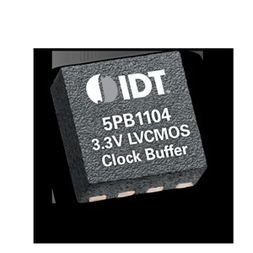
Clock Buffer 4-OUT 8-Pin DFN T/R
The 5PB1104 is a high-performance LVCMOS Clock Buffer Family. It has best-in-class Additive Phase Jitter of 50fsec RMS. There are five different fan-out variations, 1:2 to 1:10, available. The IDT5PB1104 also supports a synchronous glitch-free Output Enable function to eliminate any potential intermediate incorrect output clock cycles when enabling or disabling outputs. It comes in various packages and can operate from a 1.8V to 3.3V supply.
- High performance 1:2, 1:4, 1:6, 1:8, 1:10 LVCMOS clock buffer
- Very low pin-to-pin skew <50 ps
- Very low additive jitter <50 fs
- Supply voltage: 1.8V to 3.3V
- fMAX = 200MHz
- Integrated serial termination for 50ohm channel
- Packaged in 8-, 14-, 16-, 20-pin TSSOP and small DFN and QFN packages
- Extended (-40°C to +105°C) temperature range
Especificações
| Brand | Renesas Electronics |
|---|---|
| Number Of | 4 |
| Product description | 2 x 2 x 0.5 |
| Operating | 1.8, 2.5, 3.3 V |
| Operating temperature | -40 to 105 °C |
| Schedule B | 8542390000 |
| HTSN | 8542390001 |
| Maximum P | 2.2@1.8V|2.9@2.5V|2.4@3.3V ns |
| Supplier | DFN |
| Max Proce | 260 |
| Maximum I | 200 MHz |
| Msl Level | 1 |
| Lead Finish | Matte Tin |
SKU: 5PB1104CMGI/W