


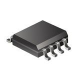
Zero Delay PLL Clock Buffer Single 8-Pin SOIC N T/R
The NB3N2302 is a versatile Zero Delay Buffer that operates from 5MHz to 133MHz with a 3.3V or 5V power supply. It accepts a reference input and drives a div 1 and a div 2 clock output. The NB3N2302 has an on-chip PLL which locks to the input reference clock presented on the REF_IN pin. The PLL feedback is required to be driven to the FBIN pin and can be obtained by connecting either the OUT1 or OUT2 pin to the FBIN pin. The Function Select inputs control the various multiplier output frequency combinations.
- Output Frequency Range: 5 MHz to 133 MHz
- Two LVTTL/LVCMOS Outputs
- 65 ps Typical Jitter OUT2
- 115 ps Typical Jitter OUT1
- Operating Voltage Range: VDD = 3.3V +/-5% or 5V +/-10%
- -40°C to +85°C Ambient Operating Temperature Range
Характеристики
| Бренд | ON Semiconductor |
|---|---|
| Описание продукта | 5 x 4 x 1.5 mm |
| Operating | 3.3, 5 V |
| Рабочая температура | -40 to 85 °C |
| Schedule B | 8542390000 |
| HTSN | 8542390001 |
| Supplier | SOIC N |
| Maximum I | 133 MHz |
| Msl Level | 1 |
| Страна происхождения | United States |
| Screening Level | Industrial |
| Minimum I | 5 MHz |
| Number Of | 1 |
| Type Prod | Zero Delay PLL Clock Buffer |
| Output Fr | 10, 133 MHz |
SKU: NB3N2302DR2G