


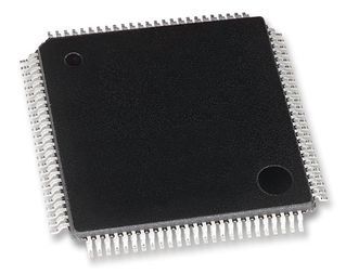
SRAM Chip Sync Quad 3.3V 2M-Bit 64K x 32 8.5ns 100-Pin TQFP
The Micron SyncBurst SRAM family employs high-speed, low-power CMOS designs that are fabricated using an advanced CMOS process. Micron’s 2Mb SyncBurst SRAMs integrate a 128K x 18, 64K x 32, or 64K x 36 SRAM core with advanced synchronous peripheral circuitry and a 2-bit burst counter. All synchronous inputs pass through registers controlled by a positive-edge-triggered single clock input (CLK). The synchronous inputs include all addresses, all data inputs, active LOW chip enable (CE#), two additional chip enables for easy depth expansion (CE2, CE2#), burst control inputs (ADSC#, ADSP#, ADV#), byte write enables (BWx#) and global write (GW#). Asynchronous inputs include the output enable (OE#), snooze enable (ZZ) and clock (CLK). There is also a burst mode pin (MODE) that selects between interleaved and linear burst modes. The data-out (Q), enabled by OE#, is also asynchronous. WRITE cycles can be from one to two bytes wide (x18) or from one to four bytes wide (x32/x36), as controlled by the write control inputs. Burst operation can be initiated with either address status processor (ADSP#) or address status controller (ADSC#) input pins. Subsequent burst addresses can be internally generated as controlled by the burst advance pin (ADV#). Address and write control are registered on-chip to simplify WRITE cycles. This allows self-timed WRITE cycles. Individual byte enables allow individual bytes to be written. During WRITE cycles on the x18 device, BWa# controls DQa pins and DQPa; BWb# controls DQb pins and DQPb. During WRITE cycles on the x32 and x36 devices, BWa# controls DQa pins and DQPa; BWb# controls DQb pins and DQPb; BWc# controls DQc pins and DQPc; BWd# controls DQd pins and DQPd. GW# LOW causes all bytes to be written. Parity bits are only available on the x18 and x36 versions. Micron’s 2Mb SyncBurst SRAMs operate from a +3.3V VDD power supply, and all inputs and outputs are TTL-compatible. Users can choose either a 3.3V or 2.5V I/O version. The device is ideally suited for 486, Pentium, 680X0, and PowerPC systems and systems that benefit from a very wide data bus. The device is also ideal in generic 16-, 18-, 32-, 36-, 64-, and 72-bit-wide applications.
- Fast clock and OE# access times
- Single +3.3V +0.3V/-0.165V power supply (VDD)
- Separate +3.3V or +2.5V isolated output buffer supply (VDDQ)
- SNOOZE MODE for reduced-power standby
- Common data inputs and data outputs
- Individual BYTE WRITE control and GLOBAL WRITE
- Three chip enables for simple depth expansion and address pipelining
- Clock-controlled and registered addresses, data I/Os and control signals
- Internally self-timed WRITE cycle
- Burst control pin (interleaved or linear burst)
- Automatic power-down
- 100-pin TQFP package
- Low capacitive bus loading
- x18, x32, and x36 versions available
Характеристики
| Бренд | Rochester Electronics |
|---|---|
| Timing Type | Synchronous |
| Number Of Words | 64 kWords |
| Density | 2 Mbit |
| Рабочая температура | 0 to 70 °C |
| Number Of Ports | 4 |
| Address B | 16 Bit |
| Number Of | 32 Bit |
| Number Of | 32 Bit |
| Maximum O | 225 mA |
| Описание продукта | 20 x 14 x 1.4 mm |
| Maximum R | 8.5 ns |
| Supplier | TQFP |
| Typical O | 3.3000 V |
| Schedule B | 8542320070 |
| HTSN | 8542320041 |
| Страна происхождения | United States |
| Screening Level | Commercial |
| Minimum O | 3.135 V |
| Maximum O | 3.6 V |
| Maximum C | 100 MHz |
| Data Rate | SDR |
| Architecture | Flow-Through |
| Lead Finish | Tin/Lead |
| Max Proce | 220 |
| Msl Level | 3|5 |
SKU: MT58L64L32FT-8.5