


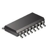
Shift Register Dual 4-Bit Serial to Parallel 16-Pin SOIC T/R
CD4015B consists of two identical, independent, 4-stage serial-input/parallel-output registers. Each register has independent CLOCK and RESET inputs as well as a single serial DATA input. "Q" outputs are available from each of the four stages on both registers. All register stages are D-type, master-slave flip-flops. The logic level present at the DATA input is transferred into the first register stage and shifted over one stage at each positive-going clock transition. Resetting of all stages is accomplished by a high level on the reset line. Register expansion to 8 stages using one CD4015B package, or to more than 8 stages using additional CD4015B’s is possible.The CD4015B-series types are supplied in 16-lead hermetic dual-in-line ceramic packages (F3A suffix), 16-lead dual-in-line plastic package (E suffix), 16-lead small-outline packages (M, M96, MT, and NSR suffixes), and 16-lead thin shrink small-outline packages (PW and PWR suffixes).
- Medium speed operation...12 MHz (typ.) clock rate at VDD – VSS = 10 V
- Fully static operation
- 8 master-slave flip-flops plus input and output buffering
- 100% tested for quiescent current at 20 V
- 5-V, 10-V, and 15-V parametric ratings
- Standardized, symmetrical output characteristics
- Maximum input current of 1 µA at 18 V over full package-temperature range; 100 nA at 18 V and 25°C
- Noise margin (full package-temperature range) =
- 1 V at VDD = 5 V
- 2 V at VDD = 10 V
- 2.5 V at VDD = 15 V
- Meets all requirements of JEDEC Tentative Standard No. 13B, "Standard Specifications for Description of ’B’ Series CMOS Devices"
Характеристики
| Бренд | Texas Instruments |
|---|---|
| Supplier | SOIC |
| Number Of | 2 |
| Lead Finish | Gold |
| Msl Level | 1 |
| Описание продукта | 10 x 4 x 1.5 mm |
| Parallel | Нет |
| Number Of | 1 |
| Direction Type | Uni-Directional |
| Operation Mode | Serial to Parallel |
| Maximum Q | 0.1 mA |
| Propagati | 50 pF |
| Maximum O | 18 V |
| Max Proce | 260 |
| Рабочая температура | -55 to 125 °C |
| Logic Function | Shift Register |
| Maximum P | 320@5V|160@10V|120@15V ns |
| Minimum O | 3 V |
| Triggering Type | Positive-Edge |
| Number Of | 4 |
| Number Of | 4 |
| Typical O | 3.3|5|9|12|15 V |
| Terminal | Нет |
| Schedule B | 8542390000 |
| HTSN | 8542390001 |
| Страна происхождения | Mexico |
SKU: CD4015BM96