


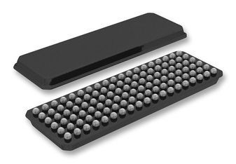
Registered Buffer Single 24-CH CMOS 114-Pin BGA MICROSTAR T/R
This 24-bit to 48-bit registered buffer is designed for 2.3-V to 2.7-V VCC operation.All inputs are SSTL_2, except the LVCMOS reset (RESET) input. All outputs are SSTL_2, Class II compatible.The SN74SSTV32852 operates from a differential clock (CLK and CLK\). Data are registered at the crossing of CLK going high and CLK\ going low.The device supports low-power standby operation. When RESET is low, the differential input receivers are disabled, and undriven (floating) data, clock, and reference voltage (VREF) inputs are allowed. In addition, when RESET is low, all registers are reset and all outputs are forced low. The LVCMOS RESET input always must be held at a valid logic high or low level.To ensure defined outputs from the register before a stable clock has been supplied, RESET must be held in the low state during power up.
Controlled Baseline Extended Temperature Performance of -40°C to 85°C Enhanced Diminishing Manufacturing Sources (DMS) Support Enhanced Product-Change Notification Qualification Pedigree(1) Member of the Texas Instruments Widebus™ Family 1-to-2 Outputs Support Stacked DDR DIMMs Supports SSTL_2 Data Inputs Outputs Meet SSTL_2 Class II Specifications Differential Clock (CLK and CLK\) Inputs Supports LVCMOS Switching Levels on the RESET\ Input RESET\ Input Disables Differential Input Receivers, Resets All Registers, and Forces All Outputs Low Pinout Optimizes DIMM PCB Layout One Device Per DIMM Required Latch-Up Performance Exceeds 100 mA Per JESD 78, Class II ESD Protection Exceeds JESD 22
- One Assembly/Test Site, One Fabrication Site
- 2000-V Human-Body Model (A114-A)
- 1000-V Charged-Device Model (C101)
Характеристики
| Бренд | Texas Instruments |
|---|---|
| Minimum O | 2.3 V |
| Lead Finish | Tin/Lead |
| Supplier | BGA MICROSTAR |
| Bus Hold | Нет |
| Msl Level | 3 |
| Polarity | Non-Inverting |
| Max Proce | 220 |
| Propagati | 30 pF |
| Описание продукта | 16 x 5.5 x 0.9 mm |
| Maximum O | 2.7 V |
| Maximum P | 3.1@2.5V ns |
| Number Of | 24 |
| Number Of | 48 |
| Number Of | 24 |
| Logic Function | Registered Buffer |
| Typical O | 2.5 V |
| Number Of | 1 |
| Triggering Type | Positive-Edge/Negative-Edge |
| Maximum L | 20 mA |
| Output Si | Single-Ended |
| Рабочая температура | -40 to 85 °C |
| Input Sig | Single-Ended |
| Maximum H | -20 mA |
| Schedule B | 8542310000 |
| HTSN | 8542390001 |
| Reset Type | Asynchronous |
| Maximum F | 200 MHz |
| Страна происхождения | United States |
SKU: CSSTV32852GKFREP