


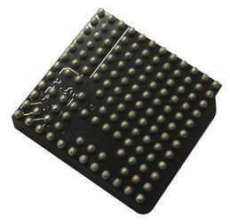
Receiver 132-Pin BGA
GD16584 is Receiver chips for use in STM-64/192 and Optical Transport Networking (OTN) systems. The component is available in two versions: GD16584 for 9.5328 Gbit/s. GD16588 for 10.66 Gbit/s for OTN or Forward Error Correction (FEC). Except the different operating bit rates the two versions are functional identical. The receiver is a Clock and Data Recovery IC with: low noise VCO Bang-Bang Phase Detector 1:16 De-multiplexer Lock Detect Phase and Frequency Detector. Clock and data are regenerated by using a Phase Locked Loop (PLL) with an external passive loop filter. The VCO frequency is controlled by one of the two Phase Detectors in order to ensure capture and lock to the line data rate. The Lock Detector circuit monitors the VCO frequency and determines when the VCO is within the lock range. When the frequency deviates more than 500 ppm from the reference clock, it automatically switches the phase and frequency detector into the PLL loop. In the auto lock mode the locking range is selectable between 500 or 2000 ppm. When the VCO frequency is within the lock range, the Bang-Bang Phase Detector takes over. It controls the phase of the VCO until the sampling point of data is in the middle of the bit period, where the eye opening is largest. A 40 mV Decision Threshold Control (DTC) is provided at the 10 Gbit/s input. The 10 Gbit/s input data is sampled and de-multiplexed by the 1:16 DeMUX. The parallel output interface is synchronised with the 622 MHz output clock. The clock and data outputs are LVDS compatible. The device operates from a dual -5.2 V and +3.3 V power supply. The power dissipation is 3.3 W, typical. The device is manufactured in a Silicon Bipolar process and packaged in an 132 ball 13 × 13 mm Ceramic/Plastic Ball Grid Array (BGA).
- Complete Clock and Data Recovery IC with auto acquisition.
- 1:16 DeMUX with differential 622 Mbit/s data outputs
- 622 MHz Clock output.
- LVDS compatible clock and data outputs.
- OIF99.102.5 compliant timing.
- 155 or 622 MHz Reference Clock.
- Input Decision Threshold Control (DTC): 40 mV.
- Low noise VCO with ±5 % tuning range.
- Dual supply operation: -5.2 V and +3.3 V.
- Power dissipation: 3.3 W (typ).
- Silicon Bipolar technology.
- Available in three package versions:
- EB: 132 ball (16 mill) Ceramic BGA 13 × 13 mm
- EF: 132 ball (20 mill) Ceramic BGA 13 × 13 mm
- FB: 132 ball (20 mill) Plastic BGA 13 × 13 mm
- Available in two versions:
- GD16584 for 10 Gbit/s
- GD16588 for 10.66 Gbit/s
Характеристики
| Бренд | Intel |
|---|---|
| Screening Level | Commercial |
| Operating | 550|140 mA |
| Typical O | -5.2, 3.3 V |
| Power Sup | Digital |
| Описание продукта | 13 x 13 x 1.22 mm |
| Рабочая температура | 0 to 70 °C |
| Schedule B | 8542390000 |
| Type Prod | Receiver |
| Category | Receiver |
| HTSN | 8542390001 |
| Страна происхождения | United States |
| Supplier | BGA |
| Lead Finish | Tin/Lead |
| Max Proce | 225 |
| Maximum O | 3.46, -4.94 V |
| Msl Level | 3|4 |
| Minimum O | 3.13, -5.46 V |
| Maximum D | 10 Gbps |
SKU: RCGD16584FB