


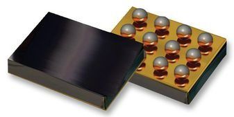
Power Switch 12-Pin WLCSP T/R
The FTL11639 is both a timer for resetting a mobile device and an advanced load management device for applications requiring a highly integrated solution. If the mobile device is off, holding /SR0 LOW (by pressing power-on key) for 38 ms ±20% turns on the PMIC. As a reset timer, it has one input and one fixed delay output. It generates a fixed delay of 11.5 s ±20% by disconnecting the PMIC from the battery power supply. FTL11639 does not accept a new input signal for 400 ms ±20% to give the PMIC enough time to turn off. The reset delay can be customized by connecting an external resistor to the DELAY_ADJ pin. As an advanced load management switch, the FTL11639 disconnects loads powered from the DC power rail (<6 V) with stringent off-state current targets and high load capacitances (up to 200 µF). The FTL11639 consists of a slew-rate controlled low-impedance MOSFET switch (21 m? typical at 4.5 V) that has exceptionally low off-state current drain (<0.2 µA typical) to facilitate compliance with standby power requirements. The slew-rate-controlled turn-on characteristic prevents inrush current and the resulting excessive voltage drop on power rails. The low ICCT enables direct interface to lower-voltage chipsets without external translation, while maintaining low power consumption. The device is packaged in advanced, fully “green,” 1.31 mm x 1.62 mm, Wafer-Level Chip-Scale Packaging (WLCSP); providing excellent thermal conductivity, small footprint, and low electrical resistance for a wide application range.
- Factory Customized Turn-on Time: 38 ms
- Factory Customized Turn-off Delay: 900 ms
- Factory Programmed Reset Delay: 11.5 s
- Factory Programmed Reset Pulse: 400 ms
- Low < 0.2 µA Typical Shutdown Current
- Off Pin Turns Off Load Switch to Maintain Battery Charge during Shipment and Inventory (Ready to Use Right Out of the Box)
- Typical RON: 21 mO (Typ.) at VBAT=4.5 V
- 3.8 A / 4.5 A Maximum Continuous Current (JEDEC 2S2P, No VIA / with Thermal VIA)
- Adjustable Reset Delay by an External Resistor (Optional)
- Low ICCT Saves Power Interfacing to Low-Voltage Chips
- Input Voltage Operating Range: 1.2 V to 5.5 V
- Over-Voltage Protection: Allow Input Pins > VBAT
- Slew Rate / Inrush Control with tR: 2.7 ms (Typical)
- Output Capacitor Discharge Function
- Zero-Second Test-Mode Enable
- IEC61000-4-2, Level 4 compliant SYS_WAKE Pin
- ESD Protected:
- 8 kV HBM ESD (per JESD22-A114)
- 10 kV HBM ESD (Pin to Pin, VBAT & VOUT)
- 2 kV CDM (per JESD22-C101)
Характеристики
| Бренд | ON Semiconductor |
|---|---|
| Schedule B | 8542390000 |
| HTSN | 8542390001 |
| Страна происхождения | United States |
| Maximum P | 410 mW |
| Supplier | WLCSP |
| Описание продукта | 1.31 x 1.62 |
| Рабочая температура | -40 to 85 °C |
| Input Voltage | 1.2 to 5.5 V |
| Switch On | 0.024 Ohm |
| Lead Finish | Tin|Silver|Copper |
| Max Proce | 260 |
| Msl Level | 1 |
| Number Of | 1 |
| Operating | 1.2, 5.5 V |
| Supply Current | 0.06 mA |
SKU: FTL11639UCX