


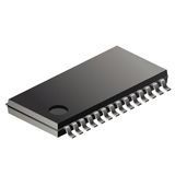
PLL Clock Generator Single 28-Pin TSSOP
The device ID (ID0 and ID1) is a part of the SMBus device 8-bit address. The least significant bit of the address designates a write or read operation. Table 2 shows the addresses for four CY24272 devices on the same SMBus. The CY24272 is a slave receiver supporting operations in the word and byte modes described in sections 5.5.4 and 5.5.5 of the SMBus Specification 2.0. DC specifications are modified to Rambus standard to support 1.8, 2.5, and 3.3 volt devices. Time out detection and packet error protocol SMBus features are not supported. Hold time for SDA is reduced relative to the CY24271, so that it is compatible with I2C.
- Meets Rambus® Extended Data Rate (XDR™) clocking requirements
- 25 ps typical cycle-to-cycle jitter
- 135 dBc/Hz typical phase noise at 20 MHz offset
- 100 or 133 MHz differential clock input
- 300-667 MHz high speed clock support
- Quad (open drain) differential output drivers
- Supports frequency multipliers: 3, 4, 5, 6, 9/2, and 15/4
- Spread Aware™
- 2.5 V operation
- 28-pin TSSOP package
Характеристики
| Бренд | Rochester Electronics |
|---|---|
| Msl Level | 1|3 |
| Рабочая температура | 0 to 70 °C |
| Schedule B | 8542310000 |
| HTSN | 8542310001 |
| Страна происхождения | United States |
| Описание продукта | 9.8 x 4.5 x 0.95 mm |
| Lead Finish | Matte Tin|Gold |
| Supplier | TSSOP |
| Max Proce | 235|260 |
| Screening Level | Commercial |
| Output Fr | 300, 667 MHz |
| Minimum I | 133 MHz |
| Operating | 2.5 V |
| Number Of | 1 |
| Type Prod | PLL Clock Generator |
SKU: CY24272ZXC