


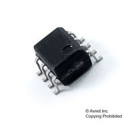
OP Amp Single GP 16V 8-Pin SOP
The TLC271 operational amplifier combines a wide range of input offset voltage grades with low offset voltage drift and high input impedance. In addition, the TLC271 offers a bias-select mode that allows the user to select the bestcombination of power dissipation and ac performance for a particular application. These devices use Texas Instruments silicon-gate LinCMOSTM technology, which provides offset voltage stability far exceeding the stability available with conventional metal-gate processes. Using the bias-select option, these cost-effective devices can be programmed to span a wide range of applications that previously required BiFET, NFET, or bipolar technology. Three offset voltage grades are available (C-suffix and I-suffix types), ranging from the low-cost TLC271 (10 mV) to the TLC271B (2 mV) low-offset version. The extremely high input impedance and low bias currents, in conjunction with good common-mode rejection and supply voltage rejection, make these devices a good choice for new state-of-the-art designs as well as for upgrading existing designs. In general, many features associated with bipolar technology are available in LinCMOSTM operational amplifiers, without the power penalties of bipolar technology. General applications such as transducer interfacing, analog calculations, amplifier blocks, active filters, and signal buffering are all easily designed with the TLC271. The devices also exhibit low-voltage single-supply operation, making them ideally suited for remote and inaccessible battery-powered applications. The common-mode input voltage range includes the negative rail. A wide range of packaging options is available, including small-outline and chip-carrier versions for high-density system applications. The device inputs and output are designed to withstand -100-mA surge currents without sustaining latch-up. The TLC271 incorporates internal ESD-protection circuits that prevent functional failures at voltages up to 2000 V as tested under MIL-STD-883C, Method 3015.2; however, care should be exercised in handling these devices as exposure to ESD may result in the degradation of the device parametric performance. The C-suffix devices are characterized for operation from 0°C to 70°C. The I-suffix devices are characterized for operation from -40°C to 85°C. The M-suffix devices are characterized for operation over the full military temperature range of -55°C to 125°C.
Input Offset Voltage Drift...Typically
0.1 uV/Month, Including the First 30 Days Wide Range of Supply Voltages Over Specified Temperature Range: 0°C to 70°C...3 V to 16 V -40°C to 85°C...4 V to 16 V -55°C to 125°C...5 V to 16 V Single-Supply Operation Common-Mode Input Voltage Range Extends Below the Negative Rail (C-Suffix and I-Suffix Types) Low Noise...25 nV/vHz Typically at
f = 1 kHz (High-Bias Mode) Output Voltage Range Includes Negative Rail High Input Impedance...1012O Typ ESD-Protection Circuitry Small-Outline Package Option Also Available in Tape and Reel Designed-In Latch-Up Immunity
0.1 uV/Month, Including the First 30 Days
f = 1 kHz (High-Bias Mode)
Характеристики
| Бренд | Texas Instruments |
|---|---|
| Рабочая температура | 0 to 70 °C |
| Shut Down | Нет |
| Operating | 1.6@5V mA |
| Typical I | 25@5V nV/rtHz |
| Maximum I | 0.00006@5V uA |
| Lead Finish | Gold |
| Operating | 16 V |
| Описание продукта | 6.2 x 5.3 x 1.95 mm |
| Power Sup | Single |
| Type Prod | General Purpose Amplifier |
| Max Proce | 260 |
| Supplier | SOP |
| Maximum I | 2@5V mV |
| Typical V | 87.23 dB |
| Msl Level | 1 |
| Typical S | 3.6@5V V/us |
| Number Of | 1 |
| Maximum O | 16 V |
| Minimum Cmrr | 65 dB |
| Schedule B | 8542330000 |
| HTSN | 8542330001 |
| Страна происхождения | United States |
| Maximum P | 1000 mW |
| Typical G | 1.7 MHz |
| Technology | LinCMOS |
SKU: TLC271BCPS