


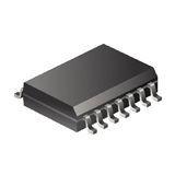
LVDS 0.65V 14-Pin SOIC N
The DS91D180 and DS91C180 are 100 MHz M-LVDS (Multipoint Low Voltage Differential Signaling) line driver/receiver pairs designed for applications that utilize multipoint networks (e.g. clock distribution in ATCA and uTCA based systems). M-LVDS is a bus interface standard (TIA/EIA-899) optimized for multidrop networks. Controlled edge rates, tight input receiver thresholds and increased drive strength are sone of the key enhancments that make M-LVDS devices an ideal choice for distributing signals via multipoint networks.The DS91D180/DS91C180 driver input accepts LVTTL/LVCMOS signals and converts them to differential M-LVDS signal levels. The DS91D180/DS91C180 receiver accepts low voltage differential signals (LVDS, B-LVDS, M-LVDS, LV-PECL and CML) and converts them to 3V LVCMOS signals. The DS91D180 device has a M-LVDS type 1 receiver input with no offset.The DS91C180 device has a type 2 receiver input which enable failsafe functionality.
DC to 100+ MHz / 200+ Mbps Low Power, Low EMI Operation Optimal for ATCA, uTCA Clock Distribution Networks Meets or Exceeds TIA/EIA-899 M-LVDS Standard Wide Input Common Mode Voltage for Increased Noise Immunity DS91D180 has Type 1 Receiver Input DS91C180 has Type 2 Receiver Input for Fail-Safe Functionality Industrial Temperature Range Space Saving SOIC-14 Package (JEDEC MS-012)
Характеристики
| Бренд | Texas Instruments |
|---|---|
| Maximum O | 3.6 V |
| Maximum P | 5.5 ns |
| Minimum O | 3 V |
| Supplier | SOIC N |
| Lead Finish | Tin |
| Описание продукта | 8.64 x 3.91 x 1.45 mm |
| Max Proce | 260 |
| Msl Level | 1 |
| Number Of | 2 |
| Number Of | 2 |
| Рабочая температура | -40 to 85 °C |
| Typical O | 3.3 V |
| Number Of | 2 |
| Input Type | LVCMOS|LVTTL|MLVDS |
| Schedule B | 8542390000 |
| HTSN | 8542390001 |
| Страна происхождения | United States |
| Transmiss | 200 Mbps |
| Screening Level | Industrial |
| Maximum P | 1100 mW |
SKU: DS91C180TMA/NOPB