


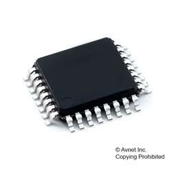
Low Voltage/Low Skew,1:8 PCI/PCI-X Zero Delay Clock Generator
The 87608I has a selectable REF_CLK or crystal input. The REF_CLK input accepts LVCMOS or LVTTL input levels. The 87608I has a fully integrated PLL along with frequency confi gurable clock and feedback outputs for multiplying and regenerating clocks with "zero delay". The 87608I is a 1:8 PCI/PCI-X Clock Generator. . The 87608I has a selectable REF_CLK or crystal input. The REF_CLK input accepts LVCMOS or LVTTL input levels. The 87608I has a fully integrated PLL along with frequency confi gurable clock and feedback outputs for multiplying and regenerating clocks with "zero delay". The PLL’s VCO has an operating range of 250MHz- 500MHz, allowing this device to be used in a variety of general purpose clocking applications. For PCI/PCI-X applications in particular, the VCO frequency should be set to 400MHz. This can be accomplished by supplying 33.33MHz, 25MHz, 20MHz, or 16.66MHz on the reference clock or crystal input and by selecting ÷12, ÷16, ÷20, or ÷24, respectively as the feedback divide value. The dividers on each of the two output banks can then be independently confi gured to generate 33.33MHz (÷12), 66.66MHz (÷6), 100MHz (÷4), or 133.33MHz (÷3). The 87608I is characterized to operate with its core supply at 3.3V and each bank supply at 3.3V or 2.5V. The 87608I is packaged in a small 7x7mm body LQFP, making it ideal for use in space-constrained applications.
- Fully integrated PLL
- Eight LVCMOS/LVTTL outputs, 15O typical output impedance
- Selectable crystal oscillator interface or LVCMOS/LVTTL REF_IN clock input
- Maximum output frequency: 166.67MHz
- Maximum crystal input frequency: 38MHz
- Maximum REF_IN input frequency: 41.67MHz
- Individual banks with selectable output dividers for generating 33.333MHz, 66.66MHz, 100MHz and 133.333MHz
- Separate feedback control for generating PCI / PCI-X frequencies from a 16.66MHz or 20MHz crystal, or 25MHz or 33.33MHz reference frequency
- VCO range: 200MHz to 500MHz
- Cycle-to-cycle jitter: 120ps (maximum), @ 3.3V
- Period jitter, RMS: 20ps (maximum)
- Output skew: 250ps (maximum)
- Bank skew: 60ps (maximum)
- Static phase offset: 160ps ± 160ps
- Voltage Supply Modes: VDD (core/inputs), VDDA (analog supply for PLL), VDDOA (output bank A), VDDOB (output bank B, REF_OUT, FB_OUT)
- -40°C to 85°C ambient operating temperature
- Available in lead-free RoHS compliant package
Характеристики
| Бренд | Renesas Electronics |
|---|---|
| Msl Level | 3 |
| Рабочая температура | -40 to 85 °C |
| Schedule B | 8542390000 |
| HTSN | 8542390001 |
| Страна происхождения | Philippines |
| Описание продукта | 7 x 7 x 1.4 mm |
| Lead Finish | Matte Tin |
| Supplier | LQFP |
| Max Proce | 260 |
| Screening Level | Industrial |
| Ширина | 7 mm |
| Pitch | 0.8 |
| Длина | 7 |
| Maximum I | 41.67 MHz |
| Output Fr | 166.67 MHz |
| Minimum I | 8.33 MHz |
| Operating | 3.3 V |
| Number Of | 1 |
| Type Prod | Zero Delay PLL Clock Generator |
SKU: 87608AYILF