


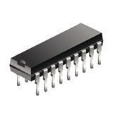
Latch/Decoder/Driver Single 4-to-7 18-Pin PDIP Rail
The MC14513B BCD-to-seven segment latch/decoder/driver is constructed with complementary MOS (CMOS) enhancement mode devices and NPN bipolar output drivers in a single monolithic structure. The circuit provides the functions of a 4-bit storage latch, an 8421 BCD-to-seven segment decoder, and has output drive capability. Lamp test (LT), blanking (BI), and latch enable (LE) inputs are used to test the display, to turn-off or pulse modulate the brightness of the display, and to store a BCD code, respectively. The Ripple Blanking Input (RBI) and Ripple Blanking Output (RBO) can be used to suppress either leading or trailing zeroes. It can be used with seven-segment light emitting diodes (LED), incandescent, fluorescent, gas discharge, or liquid crystal readouts either directly or indirectly.
- Low Logic Circuit Power Dissipation
- High-Current Sourcing Outputs (Up to 25 mA)
- Latch Storage of Binary Input
- Blanking Input
- Lamp Test Provision
- Readout Blanking on all Illegal Input Combinations
- Lamp Intensity Modulation Capability
- Time Share (Multiplexing) Capability
- Adds Ripple Blanking In, Ripple Blanking Out to MC14511B
- Supply Voltage Range = 3.0 V to 18 V
- Capable of Driving Two Low-Power TTL Loads, One Low-Power Schottky TTL Load to Two HTL Loads Over the Rated Temperature Range
- These Devices are Pb-Free and are RoHS Compliant
Характеристики
| Бренд | ON Semiconductor |
|---|---|
| Number Of | 7 |
| Maximum P | 1440@5V|580@10V|400@15V ns |
| Number Of | 1 |
| Описание продукта | 23.24 x 6.6 x 3.55 mm |
| Polarity | Non-Inverting |
| Supplier | PDIP |
| Lead Finish | Matte Tin |
| Screening Level | Extended Industrial |
| Maximum Q | 0.02 mA |
| Propagati | 50 pF |
| Maximum O | 18 V |
| Рабочая температура | -55 to 125 °C |
| Minimum O | 3 V |
| Number Of | 1 |
| Maximum H | -0.81(Min) mA |
| Typical O | 3.3|5|9|12|15 V |
| Maximum L | 4.2(Min) mA |
| Number Of | 4 |
| Logic Function | Latch/Decoder/Driver |
| Schedule B | 8542390000 |
| HTSN | 8542390001 |
| Страна происхождения | United States |
SKU: MC14513BCPG