


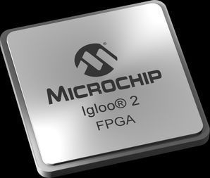
IGLOO 2
Microsemi IGLOO 2 FPGAs integrate fourth generation flash-based FPGA fabric and high-performance communications interfaces on a single chip. The IGLOO2 family is the industry’s lowest power, most reliable and highest security programmable logic solution. This next generation IGLOO2 architecture offers up to 3.6X gate count implemented with 4-input look-up table (LUT) fabric with carry chains, giving 2X performance, and includes multiple embedded memory options and math blocks for digital signal processing (DSP). High speed serial interfaces include PCI EXPRESS (PCIe ), 10 Gbps attachment unit interface (XAUI) / XGMII extended sublayer (XGXS) plus native serialization/deserialization (SERDES) communication, while double data rate 2 (DDR2)/DDR3memory controllers provide high speed memory interfaces.
- High-Performance FPGA
- Efficient 4-Input LUTs with Carry Chains for High Performance and Low Power
- Up to 236 Blocks of Dual-Port 18 Kbit SRAM (Large SRAM) with 400 MHz Synchronous Performance (512 x36, 512 x 32, 1 Kbit x 18, 1 Kbit x 16, 2 Kbit x 9, 2 Kbit x8, 4 Kbit x 4, 8 Kbit x 2, or 16 Kbit x 1)
- Up to 240 Blocks of Three-Port 1 Kbit SRAM with 2Read Ports and 1 Write Port (micro SRAM)
- High-Performance DSP
- Up to 240 Fast Math blocks with 18 x 18 Signed Multiplication, 17 x 17 Unsigned Multiplication and44-Bit Accumulator
- High Speed Serial Interfaces
- Up to 16 SERDES Lanes, Each Supporting:
- XGXS/XAUI Extension (To Implement a 10 Gbps(XGMII) Ethernet PHY Interface)
- Native SERDES Interface Facilitates Implementation of Serial Rapid IO in Fabric or an SGMII Interface to a soft Ethernet MAC
- PCI Express (PCIe) Endpoint Controllerx1, x2, x4 Lane PCI Express Core Up to 2 Kbytes Maximum Payload Size64-/32-Bit AXI/AHB Master and Slave Interfaces to the Application Layer
- Two AHB/APB Interfaces to FPGA Fabric (Master/Slave Capable)
- Two DMA Controllers to Offload Data Transactions
- 8-Channel Peripheral DMA (PDMA) for Data Transfer Between HPMS Peripherals and Memory
- High-Performance DMA (HPDMA) for Data Transfer Between eSRAM and DDR Memories
- High Speed Memory Interfaces
- Up to 2 High Speed DDRx Memory Controllers
- HPMS DDR (MDDR) and Fabric DDR (FDDR)Controllers
- Supports LPDDR/DDR2/DDR3
- Maximum 333 MHz Clock Rate
- SECDED Enable/Disable Feature
- Supports Various DRAM Bus Width Modes, x8, x9,x16, x18, x32, x36
- Supports Command Reordering to Optimize Memory Efficiency
- Supports Data Reordering, Returning Critical Word First for Each Command
- SDRAM Support through a Soft SDRAM Memory Controller
- High-Performance Memory Subsystem
- 64 KB Embedded SRAM (eSRAM)
- Up to 512 KB Embedded Non volatile Memory (eNVM)
- One SPI/COMM_BLK
- DDR Bridge (2 Port Data R/W Buffering Bridge to DDR Memory) with 64-Bit AXI Interface
- Non-Blocking, Multi-Layer AHB Bus Matrix Allowing Multi-Master Scheme Supporting 5 Masters and 7Slaves
- Supply-Chain Assurance Device Certificate
- Enhanced Anti-Tamper Features
- Zeroization
- Data Security Features (available on premium devices)
- Non-Deterministic Random Bit Generator (NRBG)
- User Cryptographic Services (AES-256, SHA-256,Elliptical Curve Cryptographic (ECC) Engine)
Характеристики
| Бренд | Microchip |
|---|---|
| Schedule B | 8542310000 |
| HTSN | 8542310001 |
| In System | Да |
SKU: M2GL005S-VF256