


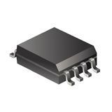
I2C Bus Repeater 8-Pin SOIC T/R
This dual bidirectional I2C buffer is operational at 2.7 V to 5.5 V. The PCA9517 is a BiCMOS integrated circuit intended for I2C bus and SMBus systems. It can also provide bidirectional voltage-level translation (up-translation/down-translation) between low voltages (down to 0.9 V) and higher voltages (2.7 V to 5.5 V) in mixed-mode applications. This device enables I2C and similar bus systems to be extended, without degradation of performance even during level shifting. The PCA9517 buffers both the serial data (SDA) and the serial clock (SCL) signals on the I2C bus, thus allowing two buses of 400-pF bus capacitance to be connected in an I2C application. This device can also be used to isolate two halves of a bus for voltage and capacitance. The PCA9517 has two types of drivers—A-side drivers and B-side drivers. All inputs and I/Os are overvoltage tolerant to 5.5 V, even when the device is unpowered (VCCB and/or VCCA = 0 V). The PCA9517 doesnot support clock stretching and arbitration across the repeater. The B-side drivers operate from 2.7 V to 5.5 V and behave like the drivers in the PCA9515A. The output low level for this internal buffer is approximately 0.5 V, but the input voltage must be 70 mV or more below the output low level when the output internally is driven low. The higher-voltage low signal is called a buffered low. When the B-side I/O is driven low internally, the low is not recognized as a low by the input. This feature prevents a lockup condition from occurring when the input low condition is released. This type of design on the B side prevents it from being used in series with the PCA9515A and another PCA9517 (B side). This is because these devices do not recognize buffered low signals as a valid low and do not propagate it as a buffered low again. The A-side drivers operate from 0.9 V to 5.5 V and drive more current. They do not require the buffered low feature (or the static offset voltage). This means that a low signal on the B side translates to a nearly 0-V low on the A side, which accommodates smaller voltage swings of lower-voltage logic. The output pulldown on the A side drives a hard low, and the input level is set at 0.3 VCCA to accommodate the need for a lower low level in systems where the low-voltage-side supply voltage is as low as 0.9 V.
Two-Channel Bidirectional Buffer I2C Bus and SMBus Compatible Operating Supply Voltage Range of 0.9 V to 5.5 V on A Side Operating Supply Voltage Range of 2.7 V to 5.5 V on B Side Voltage-Level Translation From 0.9 V to 5.5 V and 2.7 V to 5.5 V Footprint and Function Replacement for PCA9515A Active-High Repeater-Enable Input Open-Drain I2C I/O 5.5-V Tolerant I2C and Enable Input Support Mixed-Mode Signal Operation Lockup-Free Operation Accommodates Standard Mode and Fast Mode I2C Devices and Multiple Masters Powered-Off High-Impedance I2C Pins 400-kHz Fast I2C Bus Latch-Up Performance Exceeds 100 mA Per JESD 78, Class II ESD Protection Exceeds JESD 22
- 2000-V Human-Body Model (A114-A)
- 200-V Machine Model (A115-A)
- 1000-V Charged-Device Model (C101)
Характеристики
| Бренд | Texas Instruments |
|---|---|
| Max Proce | 260 |
| Supplier | SOIC |
| Рабочая температура | -40 to 85 °C |
| Category | I2C Bus Repeater |
| Описание продукта | 5 x 4 x 1.5 mm |
| Schedule B | 8542390000 |
| HTSN | 8542390001 |
| Lead Finish | Gold |
| Страна происхождения | Malaysia |
| Msl Level | 1 |
SKU: PCA9517DR