


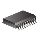
Flip Flop D-Type Bus Interface Pos-Edge 1-Element 20-Pin SOIC T/R
These devices are positive-edge-triggered D-type flip-flops with a common enable input. The ’HCT273 devices are similar to the ’HCT377 devices, but feature a common clear enable (CLR)\ input instead of a latched clock. Information at the data (D) inputs meeting the setup time requirements is transferred to the Q outputs on the positive-going edge of the clock (CLK) pulse. Clock triggering occurs at a particular voltage level and is not directly related to the positive-going pulse. When CLK is at either the high or low level, the D input has no effect at the output. The circuits are designed to prevent false clocking by transitions at (CLR)\.
Operating Voltage Range of 4.5 V to 5.5 V Outputs Can Drive Up To 10 LSTTL Loads Low Power Consumption, 80-µA Max ICC Typical tpd = 12 ns ±4-mA Output Drive at 5 V Low Input Current of 1 µA Max Inputs Are TTL-Voltage Compatible Contain Eight D-Type Flip-Flops Direct Clear Input Applications Include:
- Buffer/Storage Registers
- Shift Registers
- Pattern Generators
Характеристики
| Бренд | Texas Instruments |
|---|---|
| Описание продукта | 12.8 x 7.52 x 2.35 mm |
| Maximum H | -4 mA |
| Bus Hold | Нет |
| Polarity | Non-Inverting |
| Set Reset | Master Reset |
| Number Of | 8 |
| Number Of | 8 |
| Triggering Type | Positive-Edge |
| Рабочая температура | -40 to 85 °C |
| Input Sig | Single-Ended |
| Maximum L | 4 mA |
| Number Of | 1 |
| Maximum O | 5.5 V |
| Maximum Q | 0.008 mA |
| Output Si | Single-Ended |
| Logic Function | D-Type Bus Interface |
| Number Of | 8 |
| Minimum O | 4.5 V |
| Lead Finish | Gold |
| Supplier | SOIC |
| Max Proce | 260 |
| Typical O | 5 V |
| Msl Level | 1 |
| Schedule B | 8542390000 |
| HTSN | 8542390001 |
| Страна происхождения | Malaysia |
| Screening Level | Commercial |
SKU: SN74HCT273DWR