


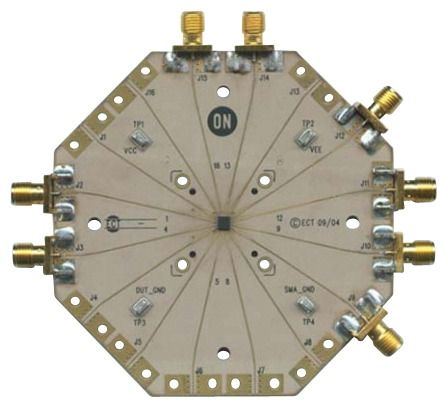
Evaluation Board For NB4N527S
NB4N527S is a clock or data Receiver/Driver/Buffer/Translator capable of translating AnyLevel input signal (LVPECL,CML, HSTL,LVDS,orLVTTL/LVCMOS)toLVDS. Depending on the distance, noise immunity of the system design, and transmission line media, this device will receive, drive or translate data or clock signals up to 2.5 Gb/s or 1.25 GHz, respectively.TheNB4N527S hasawideinputcommon mode range of GND+50 mV to VCC-50 mV combined with two 50 O internal terminationresistorsisidealfortranslatingdifferential or single-ended data or clock signals to 350 mV typical LVDS output levels without use of any additional external components.The device is offered in a small 3 mm x 3 mm QFN-16 package. NB4N527S is targeted for data, wireless and telecom applications as well as high speed logic interface where jitter and package size are main requirements.
- Maximum Input Clock Frequency up to 1.25 GHz
- Maximum Input Data Rate up to 2.5 Gb/s
- 500 ps Maximum Propagation Delay
- 2 ps Maximum RMS Jitter
- 300 ps Maximum Rise/Fall Times
- Single Power Supply; VCC = 3.3 V +/- 10%
- Temperature Compensated TIA/EIA644 Compliant LVDS Outputs
- Internal 50Termination Resistor per Input Pin
- GND + 50 mV to VCC50 mV VCMR Range
Характеристики
| Бренд | ON Semiconductor |
|---|---|
| Type Prod | Clock and Timing Tools |
| Category | Clock and Timing Tools |
| Schedule B | 8542390000 |
| HTSN | 8542390001 |
| Страна происхождения | United States |
| Описание продукта | mm |
SKU: NB4N527SMNEVB