


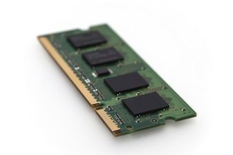
DRAM Module DDR2 SDRAM 512Mbyte 240RDIMM
DDR2 SDRAM modules are high-speed, CMOS dynamic random access memory modules that use internally configured 4 or 8-bank DDR2 SDRAM devices. DDR2 SDRAM modules use DDR architecture to achieve high-speed operation. DDR2 architecture is essentially a 4n-prefetch architecture with an interface designed to transfer two data words per clock cycle at the I/O pins. A single read or write access for the DDR2 SDRAM module effectively consists of a single 4n-bit-wide, one-clock-cycle data transfer at the internal DRAM core and eight corresponding n-bit-wide, one-half-clock-cycle data transfers at the I/O pins. DDR2 modules use two sets of differential signals: DQS, DQS# to capture data and CK and CK# to capture commands, addresses, and control signals. Differential clocks and data strobes ensure exceptional noise immunity for these signals and provide precise crossing points to capture input signals. A bidirectional data strobe (DQS, DQS#) is transmitted externally, along with data, for use in data capture at the receiver. DQS is a strobe transmitted by the DDR2 SDRAM device during READs and by the memory controller during WRITEs. DQS is edge-aligned with data for READs and center-aligned with data for WRITEs. DDR2 SDRAM modules operate from a differential clock (CK and CK#); the crossing of CK going HIGH and CK# going LOW will be referred to as the positive edge of CK. Commands (address and control signals) are registered at every positive edge of CK. Input data is registered on both edges of DQS, and output data is referenced to both edges of DQS, as well as to both edges of CK.
- 240-pin, registered dual in-line memory module
- Fast data transfer rates: PC2-3200, PC2-4200, PC2-5300, or PC2-6400
- 256MB (32 Meg x 72), 512MB (64 Meg x 72), or 1GB (128 Meg x 72)
- Supports ECC error detection and correction
- VDD = VDDQ = 1.8V
- VDDSPD = 1.7–3.6V
- JEDEC-standard 1.8V I/O (SSTL_18-compatible)
- Differential data strobe (DQS, DQS#) option
- 4n-bit prefetch architecture
- Multiple internal device banks for concurrent operation
- Programmable CAS# latency (CL)
- Posted CAS# additive latency (AL)
- WRITE latency = READ latency - 1 tCK
- Programmable burst lengths (BL): 4 or 8
- Adjustable data-output drive strength
- 64ms, 8192-cycle refresh
- On-die termination (ODT)
- Serial presence-detect (SPD) with EEPROM
- Single rank
- Gold edge contacts
Характеристики
| Бренд | Micron |
|---|---|
| Schedule B | 8473300002 |
| HTSN | 8473301180 |
| Typical O | 1.8000 V |
| Module Type | 240RDIMM |
| Maximum C | 667 MHz |
| Organization | 64Mx72 |
| Total Density | 512 MB |
| Sub Category | DDR2 SDRAM |
| Supplier | RDIMM |
| Data Bus Width | 72 Bit |
| Main Category | DRAM Module |
| Описание продукта | 133.5 x 2.7 x 30.5 mm |
| Number Of | 9 |
| Lead Finish | Gold |
| Chip Density | 512 Mb |
| Рабочая температура | 0 to 70 °C |
SKU: MT9HTF6472PZ-667G1