


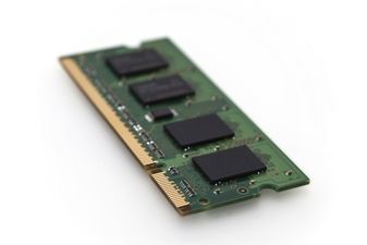
DRAM Module DDR SDRAM 512Mbyte 200SODIMM Tray
The Micron MT9VDDT6472PH is high-speed CMOS, dynamic random-access, 128MB, 256MB, 512MB, and 1GB memory modules organized in x72 (ECC) configuration. DDR SDRAM modules use internally configured quad-bank DDR SDRAM devices. DDR SDRAM modules use a double data rate architecture to achieve high-speed operation. The double data rate architecture is essentially a 2n-prefetch architecture with an interface designed to transfer two data words per clock cycle at the I/O pins. A single read or write access for the DDR SDRAM module effectively consists of a single 2n-bit wide, one-clock-cycle data transfer at the internal DRAM core and two corresponding nbit wide, one-half-clock-cycle data transfers at the I/O pins. A bidirectional data strobe (DQS) is transmitted externally, along with data, for use in data capture at the receiver. DQS is an intermittent strobe transmitted by the DDR SDRAM device during READs and by the memory controller during WRITEs. DQS is edge-aligned with data for READs and center-aligned with data for WRITEs. DDR SDRAM modules operate from differential clock inputs (CK and CK#); the crossing of CK going HIGH and CK# going LOW will be referred to as the positive edge of CK. Commands (address and control signals) are registered at every positive edge of CK. Input data is registered on both edges of DQS, and output data is referenced to both edges of DQS, as well as to both edges of CK. A phase-lock loop (PLL) device on the module is used to redrive the differential clock signals to the DDR SDRAM devices to minimize system clock loading. Read and write accesses to DDR SDRAM modules are burst oriented; accesses start at a selected location and continue for a programmed number of locations in a programmed sequence. Accesses begin with the registration of an ACTIVE command, which is then followed by a READ or WRITE command. The address bits registered coincident with the ACTIVE command are used to select the device bank and row to be accessed (BA0, BA1 select device bank; A0–A11 select device row for 128MB; A0–A12 select device row for 256MB and 512MB; and A0–A13 select device row for 1GB). The address bits registered coincident with the READ or WRITE command are used to select the device bank and the starting device column location for the burst access. DDR SDRAM modules provide for programmable read or write burst lengths of 2, 4, or 8 locations. An auto precharge function may be enabled to provide a self-timed row precharge that is initiated at the end of the burst access. The pipelined, multibank architecture of DDR SDRAM modules allows for concurrent operation, thereby providing high effective bandwidth by hiding row precharge and activation time. An auto refresh mode is provided, along with a power-saving power-down mode. All inputs are compatible with the JEDEC Standard for SSTL_2. All outputs are SSTL_2, Class II compatible.
- 200-pin, small-outline, dual in-line memory module (SODIMM)
- Supports ECC error detection and correction
- Fast data transfer rates: PC2100 and PC2700
- Utilizes 266 MT/s and 333 MT/s DDR SDRAM components
- 128MB (16 Meg x 72); 256MB (32 Meg x 72); 512MB (64 Meg x 72); 1GB (128 Meg x 72)
- VDD = VDDQ = +2.5V
- VDDSPD = +2.3V to +3.6V
- 2.5V I/O (SSTL_2 compatible)
- Commands entered on each positive CK edge
- DQS edge-aligned with data for READs; center aligned with data for WRITEs
- Internal, pipelined double data rate (DDR) architecture; two data accesses per clock cycle
- Four internal device banks for concurrent operation
- Programmable burst lengths: 2, 4, or 8
- Auto precharge option
- Auto Refresh and Self Refresh Modes
- 15.625µs (128MB), 7.8125µs (256MB, 512MB, 1GB) maximum average periodic refresh interval
- Serial Presence Detect (SPD) with EEPROM
- Programmable READ CAS latency
- Bidirectional data strobe (DQS) transmitted/received with data—i.e., source-synchronous data capture
- Differential clock inputs CK and CK#
- Gold edge contacts
Характеристики
| Бренд | Micron |
|---|---|
| Schedule B | 8542390000 |
| HTSN | 8542390001 |
| Typical O | 2.5000 V |
| Module Type | 200SODIMM |
| Maximum C | 333 MHz |
| Organization | 64Mx72 |
| Total Density | 512 MB |
| Sub Category | DDR SDRAM |
| Supplier | SODIMM |
| Data Bus Width | 72 Bit |
| Main Category | DRAM Module |
| Описание продукта | 67.75 x 3.8 x 31.9 mm |
| Number Of | 9 |
| Minimum O | 2.3 V |
| Lead Finish | Gold |
| Maximum O | 2.7 V |
| Chip Density | 512 Mb |
| Рабочая температура | 0 to 70 °C |
| Maximum R | 0.7 ns |
| Maximum O | 1400 mA |
| Screening Level | Commercial |
SKU: MT9VDDT6472PHY-335F2