


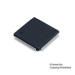
Digital Signal Processor System Memory 80-Pin TQFP
The DSM2150F5V is an 8 or 16-bit system memory device for use with the Analog Devices DSPs. DSM means Digital signal processor System Memory. A DSM device brings In-System Programmable (ISP) Flash memory, parameter storage, programmable logic, and additional I/O to DSP systems. The result is a flexible two-chip solution for DSP designs. On-chip integrated memory decode logic makes it easy to map dual banks of Flash memory to the DSPs in a variety of ways for bootloading or bypassing DSP boot ROM, code execution, data recording, code swapping, and parameter storage.JTAG ISP reduces development time, simplifies manufacturing flow, and lowers the cost of field upgrades. The JTAG ISP interface eliminates the need for sockets and pre-programmed memory and logic devices. End products may be manufactured with a blank DSM device soldered down and programmed at the end of the assembly line in 15 to 35 seconds with no involvement of the DSP. Rapidly program test code, then application code as determined by Just-In Time inventory requirements. Additionally, JTAG ISP reduces development time by turning fast iterations of DSP code in the lab. Code updates in the field require no product disassembly. The FlashLINK JTAG programming cable costs $59 USD and plugs into any PC parallel port. Programming through conventional device insertion programmers is also available using PSDpro from STMicroelectronics and other 3rd party programmers. See www.st.com/psm. DSM devices add programmable logic (PLD) and up to 32 configurable I/O pins to the DSP system. The state of I/O pins can be driven by DSP software or PLD logic. PLD and I/O configuration are programmable by JTAG ISP. The PLD consists of more than 3000 gates and has 16 macro cell registers. Common uses for the PLD include chip-selects for external devices, state-machines, simple shiftier and counters, keypad and control panel interfaces, clock dividers, handshake delay, muxes, etc., eliminating the need for small external PLDs and logic devices. Configuration of PLD, I/O, and Flash memory mapping is easily entered in a point-and-click environment using the software development tool, PSDsoft Express, available at no charge from www.st.com/psm. The two-chip DSP/DSM combination is ideal for systems having limitations on size, EMI levels, and power consumption. DSM memory and logic are “zero-power”, meaning they automatically go to standby between memory accesses or logic input changes, producing low active and standby current consumption, which is ideal for battery powered products.A programmable security bit in the DSM protects its contents from unauthorized viewing and copying. When set, the security bit will block access of programming devices (JTAG or others) to the DSM Flash memories and PLD configuration. The only way to defeat the security bit is to erase the entire DSM device, after which the device is blank and may be used again. The DSP will always have access to Flash memory contents through the data bus, even with security bit set.
- Glueless Connection to DSP
- Easily add memory, logic, and I/O to the External Port of ADSP-218x, 219x, 2106x, 2116x, 2153x, and TS101 families of DSPs from Analog Devices, Inc.
- Dual Flash Memories
- Two independent Flash memory arrays for storing DSP code and data
- Capable of read-while-write concurrent Flash memory operation
- Device can be configured as 8-bit or 16-bit
- Built-in programmable address decoding logic allows mapping individual sectors of each Flash array to any address boundary
- Each Flash sector can be write protected
- 512 KByte Main Flash memory
- Ample storage for boot loading DSP code/ data upon reset and subsequent code swaps
- Large capacity for storing tables and constants or for data recording
- 32 KByte Secondary Flash memory
- Smaller sector size ideal for storing calibration and configuration constants. Eliminate external serial EEPROM.
- Optionally bypass internal DSP boot ROM during start-up and execute code directly from Secondary Flash. Use for custom start-up code and In-Application Programming (IAP).
- Up to 40 Multifunction I/O Pins
- Increase total DSP system I/O capability
- I/O controlled by DSP software or PLD logic
- General purpose PLD
- Use for peripheral glue logic to keypads, control panel, displays, LCDs, and other devices
- Over 3,000 gates of PLD with 16 macro cells
- Eliminate PLDs and external logic devices
- Create state machines, chip selects, simple shifters and counters, clock dividers, delays
- Simple PSDsoft Express™ development software, free from www.st.com/psm
- In-System Programming (ISP) with JTAG
- Program entire chip in 15-35 seconds with no involvement of the DSP
- Optionally links with DSP JTAG debug port
- Eliminate need for sockets and preprogramming of memory and logic devices
- ISP allows efficient manufacturing and product testing supporting Just-In-Time inventory
- Use low-cost FlashLINK™ cable with any PC. Available from www.st.com/psm.
- Content Security
- Programmable Security Bit blocks access of device programmers and readers
- Operating Range
- VCC: 3.3V ± 10%, Temp: –40°C to +85°C
- Zero-Power Technology
- 50µA standby current typical
- Flash Memory Speed, Endurance, Retention
- 120ns, 100K cycles, 15 year retention
Характеристики
| Бренд | STMicroelectronics |
|---|---|
| Max Proce | 260 |
| Описание продукта | 12 x 12 x 1.05 mm |
| Lead Finish | Matte Tin |
| Msl Level | 3 |
| Supplier | TQFP |
| Рабочая температура | -40 to 85 °C |
| Schedule B | 8542310000 |
| HTSN | 8542310001 |
| Screening Level | Industrial |
| Category | Digital Signal Processor System Memory |
SKU: DSM2150F5V-12T6