


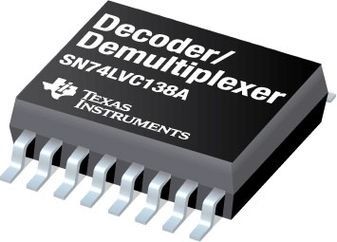
Decoder/Demultiplexer Single 3-to-8 16-Pin TSSOP T/R
The SN54LVC138A 3-line to 8-line decoder/demultiplexer is designed for 2.7-V to 3.6-V VCC operation and the SN74LVC138A 3-line to 8-line decoder/demultiplexer is designed for 1.65-V to 3.6-V VCC operation.The ’LVC138A devices are designed for highperformance memory-decoding or data-routing applications requiring very short propagation delay times. In high-performance memory systems, these decoders minimize the effects of system decoding. When employed with high-speed memories utilizing a fast enable circuit, the delay times of these decoders and the enable time of the memory are usually less than the typical access time of the memory. This means that the effective system delay introduced by the decoders is negligible.The conditions at the binary-select inputs and the three enable inputs select one of eight output lines. Two active-low enable inputs and one active-high enable input reduce the need for external gates or inverters when expanding. A 24-line decoder can be implemented without external inverters and a 32-line decoder requires only one inverter. An enable input can be used as a data input for demultiplexing applications.Inputs can be driven from either 3.3-V or 5-V devices. This feature allows the use of these devices as translators in a mixed 3.3-V/5-V system environment.The SN54LVC138A is characterized for operation over the full military temperature range of –55°C to 125°C. The SN74LVC138A is characterized for operation from –40°C to 85°C.
- EPIC(Enhanced-Performance Implanted CMOS) Submicron Process
- ESD Protection Exceeds 2000 V Per MIL-STD-883, Method 3015; Exceeds 200 V Using Machine Model (C = 200 pF, R = 0)
- Latch-Up Performance Exceeds 250 mA Per JESD 17
- Typical VOLP (Output Ground Bounce) < 0.8 V at VCC = 3.3 V, TA = 25°C
- Typical VOHV (Output VOH Undershoot) > 2 V at VCC = 3.3 V, TA = 25°C
- Inputs Accept Voltages to 5.5 V
- Package Options Include Plastic Small-Outline (D), Shrink Small-Outline (DB), and Thin Shrink Small-Outline (PW) Packages, Ceramic Chip Carriers (FK) and Flat (W) Package, and DIPs (J)
Характеристики
| Бренд | Texas Instruments |
|---|---|
| Number Of | 8 |
| Maximum P | 7.9@2.7V|6.7@3.3V ns |
| Number Of | 1 |
| Demultipl | 1-of-8 |
| Описание продукта | 5.1 x 4.5 x 1.05 mm |
| Polarity | Inverting |
| Supplier | TSSOP |
| Lead Finish | Gold |
| Msl Level | 1 |
| Maximum Q | 0.01 mA |
| Propagati | 50 pF |
| Maximum O | 3.6 V |
| Max Proce | 260 |
| Рабочая температура | -40 to 85 °C |
| Minimum O | 1.65 V |
| Number Of | 3 |
| Maximum H | -24 mA |
| Typical O | 1.8|2.5|3.3 V |
| Maximum L | 24 mA |
| Number Of | 3 |
| Logic Function | Decoder/Demultiplexer |
| Schedule B | 8542390000 |
| HTSN | 8542390001 |
| Страна происхождения | United States |
SKU: SN74LVC138APWT