


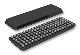
CompactFlash Interface 114-Pin BGA MICROSTAR T/R
This CompactFlash (CF) interface chip is designed to provide a single-chip solution for CF card interfaces. Separate VCC rails for the system bus side and the CF connector bus side allow voltage-level shifting. This is helpful for interfacing between a core chipset, which may operate from 3.3 V down to 1.65 V, and CF cards, which operate from 3.3-V or 5-V supply voltages. All the input buffers feature the input-disable function, which allows conditional floating input signals. The input, output, and I/O buffers on the CF connector side have been defined to comply with CF+ and CompactFlash specification revisions 1.4 and 2.0. This device has 16-bit data lines and 24-bit address/command lines. CD1\ and CD2\ have internal pullup resistors to pull them to a high logic state if there is no card in the CF slot. The presence of a CF card in the CF card slot generates a low logic signal at SCD\. A separate power-supply pin, VCC_SD, controls the SCD\ output buffer. The SCD\ signal can be used to control a voltage regulator, which may power the CF slot and the CF side of this device. VCC_SD is particularly helpful when the core processor operates at a low VCC, but the regulator needs a higher control signal voltage. The MASTER_EN\ signal controls all the buffers and transceivers except CD1\ and CD2\. If MASTER_EN\ is high, the SN74LV4320A is in a power-down mode. The BUF_EN\ signal, in conjunction with MASTER_EN\, controls the 11-bit address lines and 13-bit control/command lines. The 16-bit data lines use two separate enable signals. ENL\, in conjunction with MASTER_EN\, controls the lower 8-bit data lines (D07-D00). ENH\, in conjunction with MASTER_EN\, controls the upper 8-bit data lines (D15-D08). A DIR(S\/CF) input controls the data direction between the system bus and the CF card. An additional DIR_OUT pin generates the DIR(S\/CF) signal using the SOE and SIORD\ signals. With either SOE or SIORD\ being low, the data direction is from the CF card side to the system side (DIR_OUT = L). DIR(S\/CF) and DIR_OUT are placed adjacent to each other, which is convenient for connecting DIR(S\/CF) and DIR_OUT, if DIR_OUT is used. This saves an additional signal from the system controller to control the data direction.BVD1, BVD2, INPACK\, READY, WAIT\, and WP have 100-kO internal pullup resistors, eliminating the need for external pullups. The resistors are within the tolerance of CF+ and CompactFlash specification revisions 1.4 and 2.0. This device is fully specified for partial-power-down applications using Ioff. The Ioff circuitry disables the outputs, preventing damaging current backflow through the device when it is powered down.
Member of the Texas Instruments Widebus+™ Family Designed to Optimize Power Savings in Portable Applications 1.65-V to 5.5-V Level Translation Using Dual Supplies Matched Pinout With CompactFlash™ (CF) Connector Pin Configurations to Optimize PCB Layout Input-Disable Feature Allows Floating Input Conditions Ioff Supports Partial-Power-Down Mode Operation Latch-Up Performance Exceeds 250 mA Per JESD 17 ESD
- 15-kV Human-Body Model
- ±4-kV IEC61000-4-2, Contact Discharge (Latch-Up Immune)
Характеристики
| Бренд | Texas Instruments |
|---|---|
| Max Proce | 235 |
| Supplier | BGA MICROSTAR |
| Рабочая температура | -40 to 85 °C |
| Category | CompactFlash Interface |
| Screening Level | Commercial |
| Описание продукта | 16 x 5.5 x 0.9 mm |
| Schedule B | 8542390000 |
| HTSN | 8542390001 |
| Lead Finish | Tin/Lead |
| Страна происхождения | United States |
| Msl Level | 2 |
SKU: SN74LV4320AGKFR