


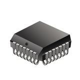
Clock Fanout Buffer 18-OUT 28-Pin PLCC T/R
The differential LVPECL clock-driver circuit distributes one pair of differential LVPECL clock inputs (CLKIN, CLKIN)\ to nine pairs of differential clock (Y, Y)\ outputs with minimum skew for clock distribution. It is specifically designed for driving 50O transmission lines.The VREF output can be strapped to the CLKIN\ input for a single-ended CLKIN input. The CDCVF111 is characterized for operation from –40°C to 85°C.
Low-Output Skew for Clock-Distribution Applications Differential Low-Voltage Pseudo-ECL (LVPECL) Compatible Inputs and Outputs Distributes Differential Clock Inputs to Nine Differential Clock Outputs Output Reference Voltage (VREF) Allows Distribution From a Single-Ended Clock Input Packaged In a 28-Pin Plastic Chip Carrier
Характеристики
| Бренд | Texas Instruments |
|---|---|
| Number Of | 18 |
| Описание продукта | 11.51 x 11.51 x 4.06 mm |
| Operating | 3.3 V |
| Maximum O | 3.6 V |
| Minimum O | 3 V |
| Schedule B | 8542390000 |
| HTSN | 8542390001 |
| Maximum P | 0.6@3.3V ns |
| Supplier | PLCC |
| Max Proce | 260 |
| Maximum I | 650 MHz |
| Msl Level | 1 |
| Lead Finish | Gold |
| Страна происхождения | United States |
| Maximum Q | 100 mA |
| Maximum P | 525 mW |
SKU: CDCVF111FNR