


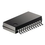
Clock Fanout Buffer 10-OUT 24-Pin SSOP T/R
The CDC2351 is a high-performance clock-driver circuit that distributes one input (A) to 10 outputs (Y) with minimum skew for clock distribution. The output-enable OE input disables the outputs to a high-impedance state. Each output has an internal series damping resistor to improve signal integrity at the load. The CDC2351 operates at nominal 3.3-V VCC. The propagation delays are adjusted at the factory using the P0 and P1 pins. The factory adjustments ensure that the part-to-part skew is minimized and is kept within a specified window. Pins P0 and P1 are not intended for customer use and should be connected to GND. The CDC2351M is characterized for operation over the full military temperature range of –55°C to 125°C.
Controlled Baseline Extended Temperature Performance of –55°C to 125°C Enhanced Diminishing Manufacturing Sources (DMS) Support Enhanced Product-Change Notification Qualification Pedigree Low Output Skew, Low Pulse Skew for Clock-Distribution and Clock-Generation Applications Operates at 3.3-V VCC LVTTL-Compatible Inputs and Outputs Supports Mixed-Mode Signal Operation (5-V Input and Output Voltages With 3.3-V VCC) Distributes One Clock Input to 10 Outputs Outputs Have Internal Series Damping Resistor to Reduce Transmission Line Effects Distributed VCC and Ground Pins Reduce Switching Noise State-of-the-Art EPIC-IIB™ BiCMOS Design Significantly Reduces Power Dissipation Shrink Small-Outline (DB) Package
- One Assembly/Test Site, One Fabrication Site
Характеристики
| Бренд | Texas Instruments |
|---|---|
| Number Of | 10 |
| Описание продукта | 8.2 x 5.3 x 1.95 mm |
| Operating | 3.3 V |
| Maximum O | 3.6 V |
| Minimum O | 3 V |
| Schedule B | 8542390000 |
| HTSN | 8542390001 |
| Maximum P | 4.8@3.3V ns |
| Supplier | SSOP |
| Max Proce | 260 |
| Maximum I | 100 MHz |
| Msl Level | 2 |
| Lead Finish | Gold |
| Страна происхождения | United States |
| Maximum Q | 15 mA |
| Maximum P | 650 mW |
SKU: CDC2351MDBREP