


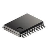
Clock Driver 2-IN LVPECL 20-Pin TSSOP
The MAX9323 low-skew, low-jitter, clock and data driver distributes one of two single-ended LVCMOS inputs to four differential LVPECL outputs. A single logic control signal (CLK_SEL) selects the input signal to distribute to all outputs. The device operates from 3.0V to 3.6V, making the device ideal for 3.3V systems, and consumes only 25mA (max) of supply current. The MAX9323 features low 150ps part-to-part skew, low 11ps output-to-output skew, and low 1.7ps RMS jitter, making the device ideal for clock and data distribution across a backplane or board. All outputs are enabled and disabled synchronously with the clock input to prevent partial output clock pulses. The MAX9323 is available in space-saving 20-pin TSSOP and ultra-small 20-pin 4mm x 4mm thin QFN packages and operates over the extended (-40°C to +85°C) temperature range. The MAX9323 is pin compatible with Integrated Circuit Systems" ICS8535-01.
- 1.7psRMS Added Random Jitter
- 150ps (max) Part-to-Part Skew
- 11ps Output-to-Output Skew
- 450ps Propagation Delay
- Pin Compatible with ICS8535-01 20-Lead TSSOP
- Consumes Only 25mA (max) Supply Current (50% Less than ICS8535-01)
- Synchronous Output Enable/Disable
- Two Selectable LVCMOS Inputs
- 3.0V to 3.6V Supply Voltage Range
- -40°C to +85°C Operating Temperature Range
Характеристики
| Бренд | Maxim Integrated |
|---|---|
| Max Proce | 260|300 |
| Supplier | TSSOP |
| Рабочая температура | -40 to 85 °C |
| Описание продукта | 6.5 x 4.4 x 0.9 mm |
| Schedule B | 8542390000 |
| HTSN | 8542390001 |
| Lead Finish | Matte Tin |
| Msl Level | 1 |
| Operating | 3.3 V |
| Maximum O | 3.6 V |
| Minimum O | 3 V |
| Input Sig | LVCMOS |
| Configuration | 1 x 2:1 |
| Operation Mode | Single-Ended |
| Power Sup | Single |
| Maximum Q | 25 mA |
| Maximum P | 879.1 mW |
SKU: MAX9323EUP+