


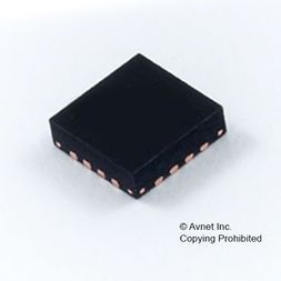
Clock Buffer/Divider 16-Pin VQFN EP T/R
The CDCM1802 clock driver distributes one pair of differential clock input to one LVPECL differential clock output pair Y0 and Y0 and one single-ended LVCMOS output Y1. It is specifically designed for driving 50-O transmission lines. The LVCMOS output is delayed by 1.6 ns over the PECL output stage to minimize noise impact during signal transitions. The CDCM1802 has two control pins, S0 and S1, to select different output mode settings. The S[1:0] pins are 3-level inputs. Additionally, an enable pin EN is provided to disable or enable all outputs simultaneously. The CDCM1802 is characterized for operation from –40°C to 85°C. For single-ended driver applications, the CDCM1802 provides a VBB output pin that can be directly connected to the unused input as a common-mode voltage reference.
Distributes One Differential Clock Input to One LVPECL Differential
Clock Output and One LVCMOS Single-Ended Output Programmable Output Divider for Both LVPECL and LVCMOS Outputs 1.6-ns Output Skew Between LVCMOS and LVPECL Transitions Minimizing Noise 3.3-V Power Supply (2.5-V Functional) Signaling Rate Up to 800-MHz LVPECL and 200-MHz LVCMOS Differential Input Stage for Wide Common-Mode Range Also Provides VBB
Bias Voltage Output for Single-Ended Input Signals Receiver Input Threshold ±75 mV 16-Pin QFN Package (3 mm × 3 mm)
Clock Output and One LVCMOS Single-Ended Output
Bias Voltage Output for Single-Ended Input Signals
Характеристики
| Бренд | Texas Instruments |
|---|---|
| Описание продукта | 3 x 3 x 0.9 mm |
| Рабочая температура | -40 to 85 °C |
| Schedule B | 8542390000 |
| HTSN | 8542390001 |
| Supplier | VQFN EP |
| Max Proce | 260 |
| Msl Level | 2 |
| Lead Finish | Gold |
| Страна происхождения | United States |
| Category | Clock Buffer/Divider |
SKU: CDCM1802RGTR