


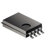
Clock Buffer/Clock Multiplier 8-Pin TSSOP Tube
The CDCS503 is a spread spectrum capable, LVCMOS Input Clock Buffer with selectable frequency multiplication. It shares major functionality with the CDCS502 but utilizes a LVCMOS input stage instead of the crystal input stage of the CDCS502. Also an Output Enable pin has been added to the CDCS503. The device accepts a 3.3V LVCMOS signal at the input. The input signal is processed by a PLL, whose output frequency is either equal to the input frequency or multiplied by the factor of 4. The PLL is also able to spread the clock signal by ±0%, ±0.5%, ±1% or ±2% centered around the output clock frequency with a triangular modulation. By this, the device can generate output frequencies between 8MHz and 108MHz with or without SSC. A separate control pin can be used to enable or disable the output. The CDCS503 operates in 3.3V environment. It is characterized for operation from –40°C to 85°C, and available in an 8-pin TSSOP package.
Part of a Family of Easy to use Clock Generator Devices
With Optional SSC Clock Multiplier With Selectable Output Frequency and
Selectable SSC SSC Controllable via 2 External Pins Frequency Multiplication Selectable Between x1 or x4
With One External Control Pin Output Disable via Control Pin Single 3.3V Device Power Supply Wide Temperature Range –40°C to 85°C Low Space Consumption by 8 Pin TSSOP Package APPLICATIONS
With Optional SSC
Selectable SSC
- ±0%, ±0.5%, ±1%, ±2% Center Spread
With One External Control Pin
- Consumer and Industrial Applications requiring
EMI reduction through Spread Spectrum Clocking
and/or Clock Multiplication
Характеристики
| Бренд | Texas Instruments |
|---|---|
| Описание продукта | 3.1 x 4.5 x 1.05 mm |
| Рабочая температура | -40 to 85 °C |
| Schedule B | 8542390000 |
| HTSN | 8542390001 |
| Supplier | TSSOP |
| Max Proce | 260 |
| Msl Level | 1 |
| Lead Finish | Gold |
| Страна происхождения | United States |
| Category | Clock Buffer/Clock Multiplier |
SKU: CDCS503PW