


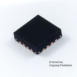
Clock Buffer 2-OUT 16-Pin QFN T/R
This 3.3V low-skew, low-jitter, precision LVDS output clock divider accepts any high-speed differential clock input (AC- or DC-coupled) CML, LVPECL, HSTL or LVDS and divides down the frequency using a programmable divider ratio to create a frequency-locked, lower speed version of the input clock. The SY89873L includes two output banks. Bank A is an exact copy of the input clock (pass through) with matched propagation delay to Bank B, the divided output bank. Available divider ratios are 2, 4, 8 and 16. In a typical 622MHz clock system this would provide availability of 311MHz, 155MHz, 77MHz or 38MHz auxiliary clock components. The differential input buffer has a unique internal termination design that allows access to the termination network through a VT pin. This feature allows the device to easily interface to all AC- or DC-coupled differential logic standards. A VREF-AC reference is included for AC-coupled applications. The SY89873L is part of Micrel’s high-speed Precision Edge® timing and distribution family. For 2.5V applications, consider the SY89872U. For applications that require an LVPECL output. The /RESET input asynchronously resets the divider outputs (Bank B). In the pass-through function (Bank A) the /RESET synchronously enables or disables the outputs on the next falling edge of IN (rising edge of /N).
Guaranteed AC performance > 2.0GHz fMAX output toggle > 3.0GHz fMAX input < 800ps tPD (matched-delay between banks) < 15ps within-device skew < 190ps rise/fall time Low jitter design < 1psRMS cycle-to-cycle jitter Unique input termination and VT pin for DC-coupled and AC-coupled inputs: any differential inputs (LVPECL, LVDS, CML, HSTL) Precision differential LVDS outputs Matched delay: all outputs have matched delay, independent of divider setting TTL/CMOS inputs for select and reset/disable Two LVDS output banks (matched delay) Bank A: Buffered copy of input clock (undivided) Bank B: Divided output (÷2, ÷4, ÷8, ÷16), two copies 3.3V power supply Wide operating temperature range: -40°C to +85°C Available in 16-pin (3mm × 3mm) QFN package
Характеристики
| Бренд | Microchip |
|---|---|
| Number Of | 2 |
| Operating | 3.3000 V |
| Maximum O | 3.3 V |
| Рабочая температура | -40 to 85 °C |
| Schedule B | 8542390000 |
| HTSN | 8542390001 |
| Maximum P | 0.8@3.3V ns |
| Maximum I | 3200 MHz |
| Msl Level | 2 |
| Страна происхождения | Malaysia |
| Maximum Q | 115 mA |
| Maximum D | 50 % |
| Family | SY89873L |
| Упаковка | Tape and Reel |
SKU: SY89873LMG-TR