


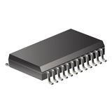
Bus XCVR Single 8-CH 3-ST 24-Pin SOIC T/R
The ’ABT853 8-bit to 9-bit parity transceivers are designed for communication between data buses. When data is transmitted from the A bus to the B bus, a parity bit is generated. When data is transmitted from the B bus to the A bus with its corresponding parity bit, the open-collector parity-error (ERR\) output indicates whether or not an error in the B data has occurred. The output-enable (OEA\ and OEB\) inputs can be used to disable the device so that the buses are effectively isolated. The ’ABT853 transceivers provide true data at their outputs. A 9-bit parity generator/checker generates a parity-odd (PARITY) output and monitors the parity of the I/O ports with the ERR\ flag. The parity-error output can be passed, sampled, stored, or cleared from the latch using the latch-enable (LE\) and clear (CLR\) control inputs. When both OEA\ and OEB\ are low, data is transferred from the A bus to the B bus and inverted parity is generated. Inverted parity is a forced error condition that gives the designer more system diagnostic capability. When VCC is between 0 and 2.1 V, the device is in the high-impedance state during power up or power down. However, to ensure the high-impedance state above 2.1 V, OE should be tied to VCC through a pullup resistor; the minimum value of the resistor is determined by the current-sinking capability of the driver.
- State-of-the-Art EPIC-??B™ BiCMOS Design Significantly Reduces Power Dissipation
- ESD Protection Exceeds 2000 V Per MIL-STD-883, Method 3015; Exceeds 200 V Using Machine Model (C = 200 pF, R = 0)
- Latch-Up Performance Exceeds 500 mA Per JESD 17
- Typical VOLP (Output Ground Bounce) < 1 V at VCC = 5 V, TA = 25°C
- High-Drive Outputs (–32-mA IOH, 64-mA IOL)
- High-Impedance State During Power Up and Power Down
- Parity-Error Flag With Parity Generator/Checker
- Latch for Storage of Parity-Error Flag
- Package Options Include Plastic Small-Outline (DW), Shrink Small-Outline (DB), and Thin Shrink Small-Outline (PW) Packages, Ceramic Chip Carriers (FK), Ceramic Flat (W) Package, and Plastic (NT) and Ceramic (JT) DIPs
Характеристики
| Бренд | Texas Instruments |
|---|---|
| Maximum Q | 38000 uA |
| Logic Function | Bus Transceiver with Parity Checker |
| Typical O | 5 V |
| Polarity | Non-Inverting |
| Max Proce | 260 |
| Propagati | 50 pF |
| Number Of | 2 Low |
| Number Of | 8 |
| Bus Hold | Нет |
| Описание продукта | 15.4 x 7.52 x 2.35 mm |
| Рабочая температура | -40 to 85 °C |
| Maximum L | 64 mA |
| Output Type | 3-State |
| Number Of | 1 |
| Output Level | TTL |
| Minimum O | 4.5 V |
| Maximum H | -32 mA |
| Supplier | SOIC |
| Msl Level | 1 |
| Maximum P | 4.8@5V ns |
| Data Flow | Bi-Directional |
| Input Level | TTL |
| Maximum O | 5.5 V |
| Lead Finish | Gold |
| Schedule B | 8542390000 |
| HTSN | 8542390001 |
| Страна происхождения | United States |
| Number Of | 1 Low |
| Typical Q | 24000 uA |
| Screening Level | Commercial |
SKU: SN74ABT853DWR