


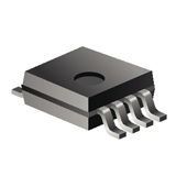
Buffer/Line Driver 2-CH Non-Inverting 3-ST CMOS 8-Pin SSOP T/R
The SN74LVC2G125-Q1 is a dual bus buffer gate designed for 1.65-V to 5.5-V VCC operation. This device features dual line drivers with 3-state outputs. The outputs are disabled when the associated output-enable (OE>) input is high. To ensure the high-impedance state during power up or power down, OE> should be tied to VCC through a pullup resistor; the minimum value of the resistor is determined by the current-sinking capability of the driver. This device is fully specified for partial-power-down applications using Ioff. The Ioff circuitry disables the outputs, preventing damaging current backflow through the device when it is powered down.
Qualified for Automotive Applications Supports 5-V VCC Operation Inputs Accept Voltages to 5.5 V Max tpd of 4.3 ns at 3.3 V Low Power Consumption, 10-µA Max ICC ±24-mA Output Drive at 3.3 V Typical VOLP (Output Ground Bounce)
<0.8 V at VCC = 3.3 V, TA = 25°C Typical VOHV (Output VOH Undershoot)
>2 V at VCC = 3.3 V, TA = 25°C Ioff Supports Partial-Power-Down Mode Operation Latch-Up Performance Exceeds 100 mA Per JESD 78, Class II
<0.8 V at VCC = 3.3 V, TA = 25°C
>2 V at VCC = 3.3 V, TA = 25°C
Характеристики
| Бренд | Texas Instruments |
|---|---|
| Output Type | 3-State |
| Typical O | 1.8|2.5|3.3|5 V |
| Minimum O | 1.65 V |
| Lead Finish | Gold |
| Maximum L | 32 mA |
| Maximum O | 5.5 V |
| Number Of | 2 |
| Polarity | Non-Inverting |
| Bus Hold | Нет |
| Описание продукта | 2.95 x 2.8 x 1.29 mm |
| Number Of | 2 |
| Number Of | 2 |
| Number Of | 2 |
| Input Sig | Single-Ended |
| Schedule B | 8542390000 |
| HTSN | 8542390001 |
| Страна происхождения | United States |
| Tolerant I Os | 5 V |
SKU: CLVC2G125IDCTRQ1