


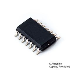
Analog Switch Quad SPST 14-Pin SOP T/R
The HCF4066B is a monolithic integrated circuit fabricated in Metal Oxide Semiconductor technology available in DIP and SOP packages.The HCF4066B is a QUAD BILATERAL SWITCH intended for the transmission or multiplexing of analog or digital signals.It is pin for pin compatible with HCF4016B, but exhibits a much lower ON resistance. In addition, the ON resistance is relatively constant over the full input signal range. The HCF4066B consists of four independent bilateral switches. A single control signal is required per switch. Both the pand n device in a given switch are biased ON or OFF simultaneously by the control signal. As shown in schematic diagram, the well of the n-channel device on each switch is either tied to the input when the switch is ON or to VSS when the switch is OFF. This configuration eliminates the variation of the switch-transistor threshold voltage with input signal, and thus keeps the ON resistance low over the full operating signal range. The advantages over single channel switches include peak input signal voltage swings equal to the full supply voltage, and more constant ON impedance over the input signal range. For sample and hold applications, however, the HCF4016B is recommended.
- 15V DIGITAL OR ± 7.5V PEAK TO PEAK SWITCHING
- 125? TYPICAL ON RESISTANCE FOR 15V OPERATION
- SWITCH ON RESISTANCE MATCHED TO WITHIN 5? TYP. OVER 15V SIGNAL INPUT RANGE
- ON RESISTANCE FLAT OVER FULL PEAK TO PEAK SIGNAL RANGE
- HIGH ON/OFF OUTPUT VOLTAGE RATIO: 65dB TYP. at fIS = 10KHz, RL = 10K?
- HIGH DEGREE OF LINEARITY: < 0.5% DISTORTION TYP. at fIS = 1KHz, VIS =5VPP, VDD - VSS > 10V, RL = 10K?
- EXTREMELY LOW OFF SWITCH LEAKAGE RESULTING IN VERY LOW OFFSET CURRENT AND HIGH EFFECTIVE OFF RESISTANCE: 10pA TYP. at VDD - VSS = 10V, Tamb = 25°C
- EXTREMELY HIGH CONTROL INPUT IMPEDANCE (control circuit isolated from signal circuit 1012? typ.)
- LOW CROSSTALK BETWEEN SWITCHES: 50dB Typ. at fIS = 0.9MHz, RL = 1K?
- MATCHED CONTROL - INPUT TO SIGNAL OUTPUT CAPACITANCE: REDUCES OUTPUT SIGNAL TRANSIENTS
- FREQUENCY RESPONSE SWITCH ON: 40MHz (Typ.)
- QUIESCENT CURRENT SPECIF. UP TO 20V
- 5V, 10V AND 15V PARAMETRIC RATINGS
Характеристики
| Бренд | STMicroelectronics |
|---|---|
| Supplier | SOP |
| Рабочая температура | -55 to 125 °C |
| Описание продукта | 8.75 x 4 x 1.65 mm |
| Operating | 20|3 V |
| Lead Finish | Tin |
| Max Proce | 260 |
| Msl Level | 1 |
| Type Prod | Analog Switch |
| Schedule B | 8542390000 |
| HTSN | 8542390001 |
| Maximum P | 200 mW |
| Output Si | Single-Ended |
| Chip Enab | Да |
| Number Of | 4 |
| Maximum O | >=1000 Ohm |
| Maximum T | 70@5V ns |
| Maximum O | 1050@5V Ohm |
| Number Of | 4 |
| Configuration | Quad SPST |
| Input Sig | Single |
| Power Sup | Single |
| Number Of | 4 |
| Polarity | Non-Inverting |
| Propagati | 50 pF |
| Maximum P | 40 ns |
SKU: HCF4066M013TR