


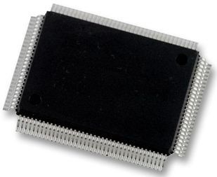
4K x 18 DualSync FIFO, 3.3V
The IDT72V845 are dual 18-bit-wide synchronous (clocked) First-in, First-out (FIFO) memories designed to run off a 3.3V supply for exceptionally low power consumption. These devices are very high-speed, low-power First-In, First-Out (FIFO) memories with clocked read and write controls. These FIFOs are applicable for a wide variety of data buffering needs, such as optical disk controllers, Local Area Networks (LANs), and interprocessor communication. Each of the two FIFOs contained in these devices has an 18-bit input and output port. Each input port is controlled by a free-running clock (WCLK), and an input enable pin (WEN). Data is read into the synchronous FIFO on every clock when WEN is asserted. The output port of each FIFO bank is controlled by another clock pin (RCLK) and another enable pin (REN). The Read Clock can be tied to the Write Clock for single clock operation or the two clocks can run asynchronous of one another for dual-clock operation. An Output Enable pin (OE) is provided on the read port of each FIFO for three-state control of the output. The synchronous FIFOs have two fixed flags, Empty Flag/Output Ready (EF/OR) and Full Flag/Input Ready (FF/IR), and two programmable flags, Almost-Empty (PAE) and Almost-Full (PAF). The offset loading of the programmable flags is controlled by a simple state machine, and is initiated by asserting the Load pin (LD). A Half-Full flag (HF) is available for each FIFO that is implemented as a single device. There are two possible timing modes of operation with these devices: IDT Standard mode and First Word Fall Through (FWFT) mode. In IDT Standard Mode, the first word written to an empty FIFO will not appear on the data output lines unless a specific read operation is performed. A read operation, which consists of activating REN and enabling a rising RCLK edge, will shift the word from internal memory to the data output lines.
- Offers optimal combination of large capacity (8K), high speed, design flexibility, and small footprint
- Ideal for the following applications:
- Network switching
- Two level prioritization of parallel data
- Bidirectional data transfer
- Bus-matching between 18-bit and 36-bit data paths
- Width expansion to 36-bit per package
- Depth expansion to 8,192 words per package
- 10 ns read/write cycle time
- 5V input tolerant
- IDT Standard or First Word Fall Through timing
- Single or double register-buffered Empty and Full Flags
- Easily expandable in depth and width
- Asynchronous or coincident Read and Write Clocks
- Asynchronous or synchronous programmable Almost-Empty and Almost-Full flags with default settings
- Half-Full flag capability
- Output enable puts output data bus in high-impedance state
- High-performance submicron CMOS technology
- Available in a 128-pin thin quad flatpack (TQFP)
- Industrial temperature range (-40°C to +85°C) is available
Характеристики
| Бренд | Renesas Electronics |
|---|---|
| Bus Directional | Bi-Directional |
| Retransmi | Нет |
| Max Proce | 260 |
| Expansion Type | Depth|Width |
| Density | 144 |
| Organization | 4Kx18x2 |
| Configuration | Quad |
| Fwft Support | Да |
| Programma | Да |
| Lead Finish | Matte Tin |
| Ширина | 14 mm |
| Supplier | TQFP |
| Msl Level | 3 |
| Expansion | Да |
| Pitch | 0.5000 |
| Длина | 20 |
| Typical O | 3.3000 V |
| Рабочая температура | 0 to 70 °C |
| Описание продукта | 20 x 14 x 1.4 mm |
| Data Bus Width | 18 Bit |
| Timing Type | Synchronous |
| Schedule B | 8542320070 |
| HTSN | 8542320071 |
| Maximum O | 60 mA |
| Maximum C | 100 MHz |
SKU: 72V845L10PFG