


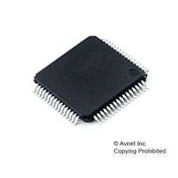
2K x 9 DualSync FIFO, 3.3V
The IDT72V831 are dual synchronous (clocked) FIFOs. Each of the two FIFOs (designated FIFO A and FIFO B) contained in the IDT72V831 has a 9-bit input data port (DA0 - DA8, DB0 - DB8) and a 9-bit output data port (QA0 - QA8, QB0 - QB8). Each input port is controlled by a free-running clock (WCLKA, WCLKB), and two Write Enable pins (WENA1, WENA2, WENB1, WENB2). Data is written into each of the two arrays on every rising clock edge of the Write Clock (WCLKA, WCLKB) when the appropriate Write Enable pins are asserted. The output port of each FIFO bank is controlled by its associated clock pin (RCLKA, RCLKB) and two Read Enable pins (RENA1, RENA2, RENB1, RENB2). The Read Clock can be tied to the Write Clock for single clock operation or the two clocks can run asynchronous of one another for dual clock operation. An Output Enable pin (OEA, OEB) is provided on the read port of each FIFO for three-state output control. Each of the two FIFOs has two fixed flags, Empty (EFA, EFB) and Full (FFA, FFB). Two programmable flags, Almost-Empty (PAEA, PAEB) and Almost-Full (PAFA, PAFB), are provided for each FIFO bank to improve memory utilization. If not programmed, the programmable flags default to Empty+7 for PAEA and PAEB, and Full-7 for PAFA and PAFB. The IDT72V831architecture lends itself to many flexible configurations such as: 2-level priority data buffering. Bidirectional operation. Width expansion. Depth expansion. This FIFO is fabricated using IDT"s high-performance submicron CMOS technology.
- Offers optimal combination of large capacity, high speed, design flexibility and small footprint
- Ideal for prioritization, bidirectional, and width expansion applications
- 10 ns read/write cycle time
- 5V input tolerant
- Separate control lines and data lines for each FIFO
- Separate Empty, Full, programmable Almost-Empty and Almost-Full flags for each FIFO
- Enable puts output data lines in high-impedance state
- Space-saving 64-pin plastic Thin Quad Flat Pack (TQFP/ STQFP)
- Industrial temperature range (-40°C to +85°C) is available
Характеристики
| Бренд | Renesas Electronics |
|---|---|
| Bus Directional | Bi-Directional |
| Maximum O | 3.6 V |
| Retransmi | Нет |
| Max Proce | 260 |
| Expansion Type | Depth|Width |
| Density | 36 |
| Organization | 2Kx9x2 |
| Configuration | Quad |
| Fwft Support | Нет |
| Programma | Да |
| Minimum O | 3 V |
| Lead Finish | Matte Tin |
| Ширина | 14 mm |
| Supplier | TQFP |
| Msl Level | 3 |
| Expansion | Да |
| Screening Level | Commercial |
| Pitch | 0.8 |
| Длина | 14 |
| Typical O | 3.3000 V |
| Рабочая температура | 0 to 70 °C |
| Описание продукта | 14 x 14 x 1.4 mm |
| Data Bus Width | 9 Bit |
| Timing Type | Synchronous |
| Schedule B | 8542320070 |
| HTSN | 8542320071 |
| Maximum O | 40 mA |
| Maximum C | 100 MHz |
SKU: 72V831L10PFG