


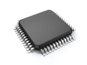
2.5V,3.3V LVCMOS Clock Fanout Buffer
The MPC9443 is a 2.5 V and 3.3 V compatible 1:16 clock distribution buffer designed for low-voltage high-performance telecom, networking and computing applications. The device supports 3.3 V, 2.5 V and dual supply voltage (mixed-voltage) applications. The MPC9443 offers 16 low-skew outputs which are divided into 4 individually configurable banks. Each output bank can be individually supplied by 2.5 V or 3.3 V, individually set to run at 1X or 1/2X of the input clock frequency or be disabled (logic low output state). Two selectable LVPECL compatible inputs support differential clock distribution systems. In addition, one selectable LVCMOS input is provided for LVCMOS clock distribution systems. The MPC9443 is specified for the extended temperature range of -40 to +85°C. The MPC9443 is a full static design supporting clock frequencies up to 350 MHz. The signals are generated and retimed on-chip to ensure minimal skew between the four output banks. Two independent LVPECL compatible clock inputs are available. This feature supports redundant differential clock sources. In addition, the MPC9443 supports single-ended LVCMOS clock distribution systems. Each of the four output banks can be individually supplied by 2.5 V or 3.3 V, supporting mixed voltage applications. The FSELx pins choose between division of the input reference frequency by one or two. The frequency divider can be set individually for each output bank. The MPC9443 output banks are in high-impedance state by deasserting the OEN pins. Asserting OEN will the enable output banks. Output High-Impedance Control (OEN) for details. The outputs can be synchronously stopped (logic low state). The outputs provide LVCMOS compatible levels with the capability to drive terminated 50 ? transmission lines. For series terminated transmission lines, each of the MPC9443 outputs can drive one or two traces giving the devices an effective fanout of 1:32 at VCC = 3.3 V. The device is packaged in a 7x7 mm² 48-lead LQFP package.
- Configurable 16 outputs LVCMOS clock distribution buffer
- Compatible to single, dual and mixed 3.3 V / 2.5 V voltage supply
- Output clock frequency up to 350 MHz
- Designed for high-performance telecom, networking and computer applications
- Supports applications requiring clock redundancy
- Maximum output skew of 250 ps (125 ps within one bank)
- Selectable output configurations per output bank
- Individually per-bank high-impedance tristate
- Output disable (stop in logic low state) control
- 48-lead LQFP package, Pb-free
- Ambient operating temperature range of -40 to 85°C
Характеристики
| Бренд | Renesas Electronics |
|---|---|
| Описание продукта | 7 x 7 x 1.4 mm |
| Operating | 2.5|3.3 V |
| Maximum O | 3.465 V |
| Minimum O | 2.375 V |
| Рабочая температура | -40 to 85 °C |
| Schedule B | 8542390000 |
| HTSN | 8542390001 |
| Supplier | TQFP |
| Max Proce | 260 |
| Pitch | 0.5000 |
| Ширина | 7 mm |
| Msl Level | 3 |
| Lead Finish | Matte Tin |
| Длина | 7 |
| Страна происхождения | Korea, South |
| Configuration | 1 x 2:1 |
| Operation Mode | Single-Ended/Differential |
| Power Sup | Single |
| Maximum O | 350 MHz |
| Input Sig | LVCMOS|LVPECL |
| Maximum Q | 3 mA |
SKU: MPC9443AE