


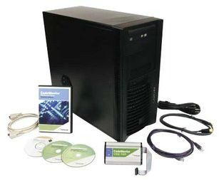
Evaluation Kit For ATX High Performance PLA
The MPC8544E PowerQUICC III is designed to offer the unique combination of high performance, exceptional integration and lower overall power consumption required for networking, communications and industrial control applications. The MPC8544E includes a high-performance e500 processor core built on Power Architecture technology, enhanced peripherals and high-speed interconnect technology to balance processor performance with I/O system throughput enabling clock speeds scaling from 667 MHz up to 1.067 GHz. Third-generation PowerQUICC III processors are based on Freescale’s 90 nanometer (nm) silicon-on-insulator (SOI) copper interconnect process technology, which is designed to enable the processors to deliver higher performance with lower power dissipation. The MPC8544E processor offers a wide range of high-speed connectivity options, including Gigabit Ethernet (GbE) interfaces with SGMII support and multiple PCI Express connections. Support for these high-speed interfaces should enable scalable connectivity to network processors and/or ASICs in the data plane while the PowerQUICC III is designed to handle complex, computationally demanding control plane processing tasks. The MPC8544E is also designed to provide support for legacy PowerQUICC III interfaces such as PCI, I²C, dual universal asynchronous receiver/transmitters (DUART) and local bus connections. These processors are also designed to feature a next-generation double data rate (DDR2) memory controller, enhanced GbE support, v2 e500 double precision floating point and the field proven 90 nm PowerQUICC III integrated security engines. Key Advantages High level of integration and performance Consistent programming model across the PowerQUICC III family Flexible SoC platform for fast time to market Simplified board design Large L2 cache at 256 KB High internal processing bandwidth Integrated DDR and DDR2 memory controller Two integrated Ethernet controllers (enhanced TSEC) with SGMII support Large L2 cache at 256 KB Flexible high-speed interconnection interfaces/multiple PCI Express connections 32-bit PCI support Integrated security engine
Embedded e500 core, initial offerings from 667 MHz up to 1.067 GHz Integrated L1/L2 cache Integrated DDR memory controller with full ECC support, offering: Integrated security engine supporting DES, 3DES, MD-5, SHA-1/2, AES, RSA, RNG, Kasumi F8/F9 and ARC-4 encryption algorithms (MPC8544E) Two on-chip enhanced triple speed Ethernet controllers (ETSECs) supporting 10 Mbps, 100 Mbps and 1 Gbps Ethernet/IEEE® 802.3 networks with MII, RMII, GMII, RGMII TBI and RTBI physical interfaces as well as SGMII interfaces through a dedicated SerDes. Enhanced hardware and software debug support Double-precision embedded scalar and vector floating-point APUs Memory management unit (MMU) PCI Express high-speed interconnect interfaces, supporting combinations of dual x4 and single x1 PCI Express On-chip network switch fabric PCI interface support Local bus Integrated four-channel DMA controller Dual I²C and DUART support Programmable interrupt controller (PIC) IEEE 1149.1 JTAG test access port 1.0V core voltage with 3.3V and 2.5V I/O 783-pin FC-PBGA package Operating junction temperature range: TJ = 0º to +105ºC, Extended temperature range: TJ = -40º to +105ºC
- Dual dispatch superscalar, 7-stage pipeline design with out-of-order issue and execution
- 2,240 MIPS at 1.0 GHz (estimated Dhrystone 2.1)
- 36-bit physical addressing
- L1 cache—32 KB data and 32 KB instruction cache with line-locking support
- L2 cache—256 KB (8-way set associative); 256/128/64/32 KB can be used as SRAM
- L1 and L2 hardware coherency
- L2 cache and I/O transactions can be stashed into L2 cache regions
- 200 MHz clock rate (400 MHz data rate), 64-bit, 2.5V/2.6V I/O, DDR SDRAM
- 267 MHz clock rate (up to 533 MHz data rate), 64-bit, 1.8V I/O, DDR2 SDRAM
- TCP/UDP/IP checksum acceleration
- Advanced QoS features
- 32-bit PCI 2.2 bus controller (up to 66 MHz, 3.3V I/O)
- 133 MHz, 32-bit, 3.3V I/O, local bus with memory controller
仕様
| Brand | NXP |
|---|---|
| Type Prod | Development Tool |
| Category | General Tools |
| Schedule B | 8471500150 |
| HTSN | 8471500150 |
| Country of origin | United States |
| Product description | mm |
SKU: MPC8544DS