


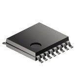
2:1 Differential Clock / Data Multiplexer
The ICS831721I is a high-performance, differential HCSL clock/data multiplexer and fanout buffer. The device is designed for the multiplexing of high-frequency clock and data signals. The device has two differential, selectable clock/data inputs. The selected input signal is output at one differential HCSL output. Each input pair accepts HCSL, LVDS, and LVPECL levels. The ICS831721I is characterized to operate from a 3.3V power supply. Guaranteed input, output-to-output and part-to-part skew characteristics make the ICS831721I ideal for those clock and data distribution applications demanding well-defined performance and repeatability. The ICS831721I supports the clock multiplexing and distribution of PCI Express Generation 1, 2 and 3 clock signals.
- 2:1 differential clock/data multiplexer with fanout
- Two selectable, differential inputs
- Each differential input pair can accept the following levels: HCSL, LVHSTL, LVDS and LVPECL
- One differential HCSL output
- Maximum input/output clock frequency: 700MHz (maximum)
- Maximum input/output data rate: 1400Mb/s (NRZ)LVCMOS interface levels for all control inputs
- Input skew: 55ps (maximum)
- Part-to-part skew: 400ps (maximum)
- Full 3.3V supply voltage
- Available in lead-free (RoHS 6) 16 TSSOP package
- -40°C to 85°C ambient operating temperature
仕様
| Brand | Renesas Electronics |
|---|---|
| Operating temperature | -40 to 85 °C |
| Configuration | 1 x 2:1 |
| Maximum O | 3.6 V |
| Supplier | TSSOP |
| Minimum O | 3 V |
| Product description | 5.1 x 4.5 x 1.05 mm |
| Schedule B | 8542390000 |
| HTSN | 8542390001 |
| Msl Level | 1 |
| Country of origin | Philippines |
| Operating | 3.3 V |
| Product width | 4.4 mm |
| Power Sup | Single |
| Pitch | 0.6500 |
| Product length | 5 |
| Maximum O | 700 MHz |
| Operation Mode | Differential |
| Input Sig | HCSL|LVDS|LVHSTL|LVPECL |
SKU: 831721AGILF