


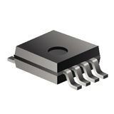
Multi Function Gate 1-Element 2-IN CMOS 8-Pin SSOP T/R
The AUP family is TI’s premier solution to the industry’s low-power needs in battery-powered portable applications. This family ensures a very low static- and dynamic-power consumption across the entire VCC range of 0.8 V to 3.6 V, resulting in an increased battery life. This product also maintains excellent signal integrity (see Figures 1 and 2).The SN74AUP1G99 features configurable multiple functions with a 3-state output. This device has the input-disable feature, which allows floating input signals. The inputs and output are disabled when the output-enable (OE) input is high. When OE is low, the output state is determined by 16 patterns of 4-bit input. The user can choose the logic functions, such as MUX, AND, OR, NAND, NOR, XOR, XNOR, inverter, and buffer. All inputs can be connected to VCC or GND.This device functions as an independent gate with Schmitt-trigger inputs, which allows for slow input transition and better switching noise immunity at the input.To ensure the high-impedance state during power up or power down, OE should be tied to VCC through a pullup resistor; the minimum value of the resistor is determined by the current-sinking capability of the driver.NanoStar and NanoFree package technology is a major breakthrough in IC packaging concepts, using the die as the package.This device is fully specified for partial-power-down applications using Ioff. The Ioff circuitry disables the outputs, preventing damaging current backflow through the device when it is powered down.
Available in the Texas Instruments
NanoFree™ Package Low Static-Power Consumption
(ICC = 0.9 µA Max) Low Dynamic-Power Consumption
(Cpd = 5 pF Typ at 3.3 V) Low Input Capacitance (CI = 1.5 pF) Low Noise – Overshoot and Undershoot
<10% of VCC Input-Disable Feature Allows Floating Input Conditions Ioff Supports Partial-Power-Down Mode Operation Includes Schmitt-Trigger Inputs Wide Operating VCC Range of 0.8 V to 3.6 V Optimized for 3.3-V Operation 3.6-V I/O Tolerant to Support Mixed-Mode Signal Operation tpd = 7.4 ns Max at 3.3 V Suitable for Point-to-Point Applications Latch-Up Performance Exceeds 100 mA Per JESD 78, Class II ESD Performance Tested Per JESD 22
NanoFree™ Package
(ICC = 0.9 µA Max)
(Cpd = 5 pF Typ at 3.3 V)
<10% of VCC
- 2000-V Human-Body Model
(A114-B, Class II) - 200-V Machine Model (A115-A)
- 1000-V Charged-Device Model (C101)
Specifications
| Brand | Texas Instruments |
|---|---|
| Maximum Q | 0.5 uA |
| Minimum O | 0.8 V |
| Lead Finish | Gold |
| Msl Level | 1 |
| Max Proce | 260 |
| Maximum O | 3.6 V |
| Maximum P | 24.9@1.2V|15.1@1.5V|11.7@1.8V|7.9@2.5V|6.7@3.3V ns |
| Product description | 2.95 x 2.8 x 1.29 mm |
| Logic Function | Multi Function |
| Operating temperature | -40 to 85 °C |
| Supplier | SSOP |
| Schedule B | 8542390000 |
| HTSN | 8542390001 |
| Country of origin | United States |
| Input Type | Schmitt Trigger |
| Screening Level | Commercial |
| Output Type | 3-State |
| Number Of | 1 |
| Number Of | 1 |
SKU: SN74AUP1G99DCTR